| Author |
Message |
ricochet
Joined: Oct 03, 2017
Posts: 4
Location: Münster, Germany
|
 Posted: Tue Nov 21, 2017 11:16 am Post subject:
vc LFO old pcb Posted: Tue Nov 21, 2017 11:16 am Post subject:
vc LFO old pcb |
  |
|
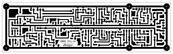
I have four of this older Yusynth vc-LFO pcb lying here to solder,
but I could'nt find any component-layout for this release..
1. Could anybody help ?
2. is this version useful or should I better stop working on that old one ?
3. are there any improvements for this pcb ?
Gerd
| Description: |
|
| Filesize: |
204.36 KB |
| Viewed: |
359 Time(s) |
| This image has been reduced to fit the page. Click on it to enlarge. |
|
| Description: |
|
| Filesize: |
88.68 KB |
| Viewed: |
366 Time(s) |
| This image has been reduced to fit the page. Click on it to enlarge. |
|
|
|
|
Back to top
|
|
 |
yusynth

Joined: Nov 24, 2005
Posts: 1314
Location: France
|
| Posted: Sun Dec 03, 2017 9:04 am Post subject:
|
|
|


_________________
Yves |
|
|
Back to top
|
|
|
yusynth
Joined: Nov 24, 2005
Posts: 1314
Location: France
|
| Posted: Sun Dec 03, 2017 9:06 am Post subject:
|
|
|


_________________
Yves |
|
|
Back to top
|
|
|
gabbagabi

Joined: Nov 29, 2008
Posts: 652
Location: Berlin by n8
Audio files: 23
|
| Posted: Tue Dec 05, 2017 8:54 am Post subject:
|
|
|
---
Last edited by gabbagabi on Tue May 18, 2021 12:52 am; edited 1 time in total |
|
|
Back to top
|
|
|
ricochet
Joined: Oct 03, 2017
Posts: 4
Location: Münster, Germany
|
| Posted: Sun Jan 21, 2018 6:52 am Post subject:
variations between layout, BOM & schematic |
|
|
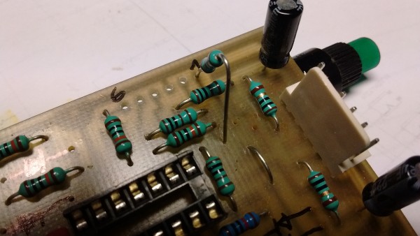
there are some questionable differences between component-layout, schematics and BoM, so, for building ready these units,
I need a little help, please...
LFO1 (A):
A1 - Capacitor C8 is shown in schematics/BoM 1nF, but in component layout 47pF ?
A2 - C5 is in BoM 10nF, but in schematics/comp-layout 100nF (I decided 100nF)
A3 - R43 (47k) isn't listet in BoM (only on the bottom of it)
A4 - as I could't find an "old" wiring pic, I see no chance of "off-board mounting the R43 resistor, so my decision is a standing mounting with
one side in hole 1 and the other side in junction R32/34 (see pic below)
LFO2 (B):
B1 - Capacitor C8 is shown in schematics/BoM 1nF, but in component layout 47pF
B2 - C5 is in BOM 10nF, but in schematics/comp-layout 100nF (I decided 100nF)
B3 - R38 isn't in BoM, maybe mistake, because there is R39 (should be R38)
B4 - C7 is in schematics/BoM & new layout, but not in the old layout and latest wiring…should I leave it or try to place it ?
B5 - R10 is shown twice in schematics (at Sin/Tri sym and at PIN 3 of IC4)... should R10 at “SinTri” named R24 ?!
B6 - R18 is shown twice in schematics (right side at PIN 5 & 7) ...R18 at PIN 7 should it be there, because PIN 7 is not connected ?!
B7 - the second side of R43 is in "wiring" connect with "pulse", but not so in schematics: there R43 is on PIN8 (IC2c) & R41…what is right ?!
thanks for your patience
Gerd
| Description: |
|
| Filesize: |
1.21 MB |
| Viewed: |
303 Time(s) |
| This image has been reduced to fit the page. Click on it to enlarge. |
|
|
|
|
Back to top
|
|
|
yusynth
Joined: Nov 24, 2005
Posts: 1314
Location: France
|
| Posted: Sun Jan 21, 2018 8:28 am Post subject:
|
|
|
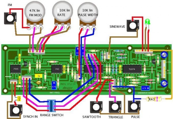
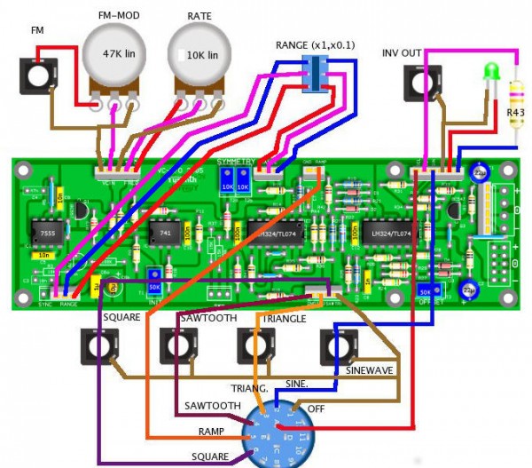
There the wiring diagrams as found on the site
| Description: |
|
| Filesize: |
118.23 KB |
| Viewed: |
310 Time(s) |
| This image has been reduced to fit the page. Click on it to enlarge. |
|
| Description: |
|
| Filesize: |
88.68 KB |
| Viewed: |
314 Time(s) |
| This image has been reduced to fit the page. Click on it to enlarge. |

|
_________________
Yves |
|
|
Back to top
|
|
|
|

 Forum index » DIY Hardware and Software » YuSynth
