| Author |
Message |
PHOBoS

Joined: Jan 14, 2010
Posts: 5884
Location: Moon Base
Audio files: 709
|
 Posted: Mon Oct 03, 2016 7:26 am Post subject:
PSK DD2000 Digital Delay - CV MOD Posted: Mon Oct 03, 2016 7:26 am Post subject:
PSK DD2000 Digital Delay - CV MOD
Subject description: adding an external CV input (+ Gate-2-Footswitch converters) |
  |
|
Years ago I got myself a PSK DD2000 Digital Delay unit, which at the time I didn't have much use for but I got it very cheap with some other gear.
Once I started making music it turned out to be a very useful effect and one of the nice features of this delay is that it has built-in modulation.
For a while I had been wondering if it would be possible to add a CV input to it for external modulation. It is afterall a pretty old delay and it
doens't use a microprocessor that could have had the modulation embedded in the code.
I am currently working on a rack for some gear which will also house this delay, so I thought now woud be a good time to see if this would be possible.
To do this I first had to figure out how the internal modulation works and since I don't have a circuit diagram this meant retracing the PCB.
Because of the layout this wasn't very easy to do but luckely I only had to figure out a small part of it before I had all the information I needed.
I had expected the DEPTH control to be an attenuator connected to GND on one side but as it turned out it actually fades between the modulation
source and a DC voltage that can be set with the FINE control.
The next thing I had to do was to see what the modulation signal looks like and what the levels of it are. So I attached my oscilloscope and
discovered a nice triangle wave oscillating between +2V and +10V. This is also how I found out that the FINE control produces a DC voltage
between +2V and +10V. So all that was needed is a circuit that converts the CV range I want to these levels and connect it to the DEPTH control
instead of the internal modulation source. However I did want the delay to still function as it is without an external modulation source and didn't
want to add a switch to the unit so I used a 1/4" connector with a switch contact.
So the circuit has to convert the CV range I want to use, which is -5V...+5V or 0..+5V, to +2V...+10V and it should not exceed this. I don't think
it would be a problem as long as it stays between 0..+12V but negative voltages could definitely damage it. Limiting the signal to +10V could
be done with a zener but the +2V is a bit trickier. I later realized that this might be possible with a 10v zenerdiode connected to +12V but what I
did instead is; first convert and limit the CV voltage to 0..5V and then adjust it to the appropriate levels.
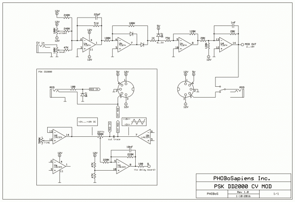
The circuit has 4 sections to achieve this:
- The first section (Ua) uses a summing amp to mix the CV, which can be attenuated, with the offset control (needed for the different CV ranges)
and an extra offset voltage to get it into the right 0...5V range.
- The second section (Ub) is an ideal diode circuit to prevent any negative voltages comming through followed by a resistor and a diode connected
to +5V to prevent it from exceeding the voltage. So after this second section the range is limited to 0..+5V no matter what I use on the input.
- The third section (Uc) amplifies the signal 1.6x to convert it to 0...+8V
- The last section (Ud) shift the voltage to the appropriate +2V..+10V range.
The circuit also needs to be powered and I didn't really want to use an external source for this, but as it turned out the delay has a build in bipolar
power supply of +/-12V and +5v as well so that was very convenient. To get access to this supply I installed a 5-pin DIN connector which also has
the internal modulation signal attached to it so I could add an external switch to still make use of it when not using the CV input.
As you can see on the photo the delay also has 2 inputs for a foot switch to control bypass and hold (turns it into a looper). So I am now thinking
about adding gate inputs for these. They are just connections to GND so I probably could get away with using a transistor, but to be safe I'd probably
use an optocoupler with either a transistor or comparator to drive it.
edit: I forgot to add the schematic
| Description: |
|
| Filesize: |
166.21 KB |
| Viewed: |
692 Time(s) |
| This image has been reduced to fit the page. Click on it to enlarge. |

|
| Description: |
|
| Filesize: |
222.49 KB |
| Viewed: |
654 Time(s) |
| This image has been reduced to fit the page. Click on it to enlarge. |

|
| Description: |
|
| Filesize: |
138.31 KB |
| Viewed: |
680 Time(s) |
| This image has been reduced to fit the page. Click on it to enlarge. |

|
| Description: |
| PSK DD2000 Digital Delay - CV MOD |
|
| Filesize: |
81.92 KB |
| Viewed: |
719 Time(s) |
| This image has been reduced to fit the page. Click on it to enlarge. |
|
_________________
"My perf, it's full of holes!"
http://phobos.000space.com/
SoundCloud BandCamp MixCloud Stickney Synthyards Captain Collider Twitch YouTube
Last edited by PHOBoS on Sun Oct 09, 2016 5:02 am; edited 1 time in total |
|
|
Back to top
|
|
 |
PHOBoS
Joined: Jan 14, 2010
Posts: 5884
Location: Moon Base
Audio files: 709
|
| Posted: Sat Oct 08, 2016 4:48 pm Post subject:
|
|
|
Made some converters to use GATE signals for the footswitch connections. The optocouplers I used (2532) where salvaged from something,
probably an old TV or PC monitor. I first tried using a CNY17 but that didn't work, these work perfect.
| Description: |
| PSK DD2000 Digital Delay - GATE-2-FOOTSWITCH converters |
|
| Filesize: |
143.34 KB |
| Viewed: |
698 Time(s) |
| This image has been reduced to fit the page. Click on it to enlarge. |

|
| Description: |
| PSK DD2000 Digital Delay - GATE-2-FOOTSWITCH converters |
|
| Filesize: |
30.25 KB |
| Viewed: |
681 Time(s) |
| This image has been reduced to fit the page. Click on it to enlarge. |

|
_________________
"My perf, it's full of holes!"
http://phobos.000space.com/
SoundCloud BandCamp MixCloud Stickney Synthyards Captain Collider Twitch YouTube |
|
|
Back to top
|
|
|
bheal
Joined: Feb 03, 2020
Posts: 1
Location: usa
|
|
|
Back to top
|
|
|
PHOBoS
Joined: Jan 14, 2010
Posts: 5884
Location: Moon Base
Audio files: 709
|
|
|
Back to top
|
|
|
|

 Forum index » DIY Hardware and Software » Stickney Synthyards


