| Author |
Message |
nullpainter

Joined: Nov 07, 2011
Posts: 32
Location: Wellington, New Zealand
|
 Posted: Sun Jan 21, 2018 10:35 pm Post subject:
[Fixed] Op amp integrator clipping Posted: Sun Jan 21, 2018 10:35 pm Post subject:
[Fixed] Op amp integrator clipping |
  |
|
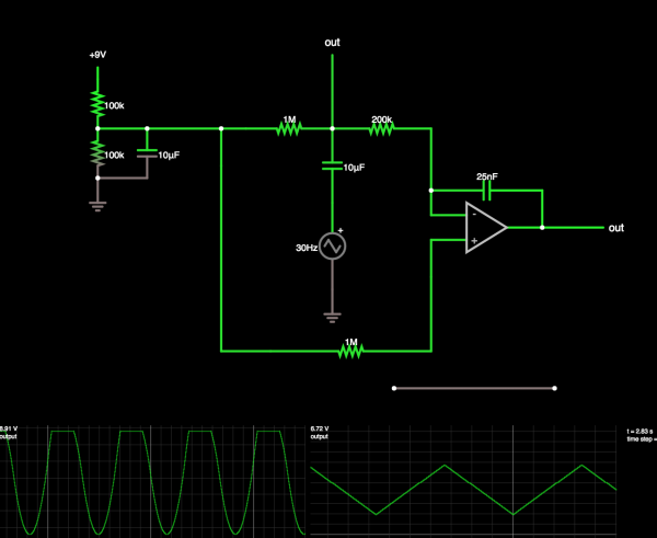
I'm building a triangle to quasi-sine wave circuit which is operating from 30Hz to 240Hz but cannot stop the output from clipping. For op amp integrator circuits, how do you control the output amplitude?
I'm using a single source 9V battery power supply and a LM386. I have simulated the circuit with the offset and peak voltage of the triangle wave as measured by my oscilloscope (output is 2.05v - 6.88v) and am seeing the same symptoms.
The output amplitude is clearly too large, but I'm not sure how to reduce it. I tried reducing the amplitude of the input triangle wave, but this resulted in saturated output. I also tried tweaking the input voltages and all other passive components but nothing is leaping out at me.
I read through Olin Lathrop's reply on elecronics.stackexchange to a regular op amp amplifier circuit to get the initial values. I increased C1 from his 10nF suggestion because the output was still fairly triangular, but I can't seem to find a happy medium between something which resembles a sine wave and an output which doesn't clip. Even C1 of ~50nF clips.
I am guessing my problems are related to C1, the biasing of my triangle wave, and the power supply circuit, but not sure how to resolve.
I am hoping for the output to be around the ~4.8V peak to peak mark to be consistent with the triangle wave, however this isn't super critical. Right now, I'm just trying to solve the clipping!
| Description: |
| Circuit from simulator, demonstrating clipped output and input signal |
|
| Filesize: |
79.67 KB |
| Viewed: |
213 Time(s) |
| This image has been reduced to fit the page. Click on it to enlarge. |
|
Last edited by nullpainter on Sat Feb 10, 2018 7:44 pm; edited 1 time in total |
|
|
Back to top
|
|
 |
JovianPyx

Joined: Nov 20, 2007
Posts: 1988
Location: West Red Spot, Jupiter
Audio files: 224
|
| Posted: Mon Jan 22, 2018 8:12 am Post subject:
|
|
|
You are using a virtual ground (network on the left) to provide a reference point yet your input is referenced to the negative side of the PSU (shown as a ground symbol). Your input signal should be referenced to the junction of the 100K resistors on the left (the virtual ground). It would help to see this if you draw it so that the virtual ground has the ground symbol instead of the negative side of the PSU (9V battery I'm guessing). This also should include relabeling of +V and -V. In reality, with this virtual ground, you have a dual voltage supply of +4.5v and -4.5v. I believe doing this will help you understand why the circuit is doing what it is.
_________________
FPGA, dsPIC and Fatman Synth Stuff
Time flies like a banana.
Fruit flies when you're having fun.
BTW, Do these genes make my ass look fat?
corruptio optimi pessima
|
|
|
Back to top
|
|
|
nullpainter
Joined: Nov 07, 2011
Posts: 32
Location: Wellington, New Zealand
|
| Posted: Mon Jan 22, 2018 11:28 pm Post subject:
|
|
|
Thanks for that. That doesn't quite make conceptual sense to me yet, so I think I need to revisit op amps and virtual grounds.
Also, I think that's just an artefact of the simulated circuit confusing things - in reality, the triangle wave is the output of another op amp inverter. I tried putting the whole circuit into that little simulator, but I think I overwhelmed it!
Will try again in Spice and report back. Thanks again for your feedback. |
|
|
Back to top
|
|
|
nullpainter
Joined: Nov 07, 2011
Posts: 32
Location: Wellington, New Zealand
|
| Posted: Thu Jan 25, 2018 11:40 pm Post subject:
|
|
|
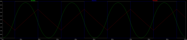
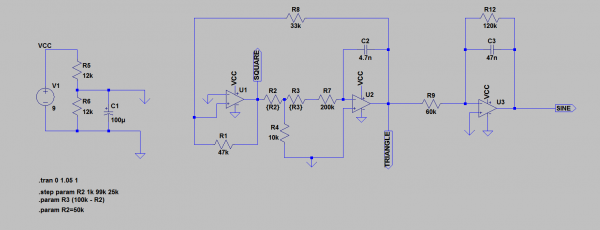
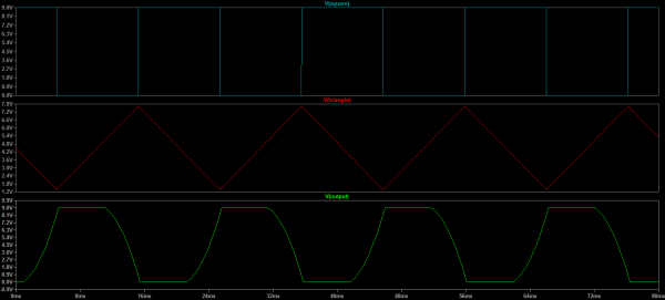
I've simulated the full circuit with LTSpice and attached an image of the circuit, and the the square, triangle and clipped sinusoidal output.
The triangle wave integrator - basically, everything to the left of R9 - is from someone else's circuit. As you can see, it works beautifully.
I just naively doubled the integrator component (R9, C3 and U3) in an attempt to transform the triangle wave into a sinusoidal wave, and that's where I'm striking problems.
A bog standard RC circuit instead of the second integrator naturally works fine.
Any pointers as to what I'm doing wrong would be greatly appreciated!
| Description: |
|
| Filesize: |
20.25 KB |
| Viewed: |
250 Time(s) |
| This image has been reduced to fit the page. Click on it to enlarge. |

|
| Description: |
|
| Filesize: |
27.02 KB |
| Viewed: |
269 Time(s) |
| This image has been reduced to fit the page. Click on it to enlarge. |
|
|
|
|
Back to top
|
|
|
nullpainter
Joined: Nov 07, 2011
Posts: 32
Location: Wellington, New Zealand
|
| Posted: Fri Jan 26, 2018 12:22 am Post subject:
|
|
|
| Actually, I just bumped up R9 and everything looks fine, in Spice at least. It's not looking fine with my circuit proper, so will double-check I haven't done something daft! |
|
|
Back to top
|
|
|
Grumble

Joined: Nov 23, 2015
Posts: 1294
Location: Netherlands
Audio files: 30
|
| Posted: Fri Jan 26, 2018 12:38 am Post subject:
|
|
|
Where does the arrow on the -input of U1 go to?
_________________
my synth |
|
|
Back to top
|
|
|
nullpainter
Joined: Nov 07, 2011
Posts: 32
Location: Wellington, New Zealand
|
| Posted: Fri Jan 26, 2018 2:10 am Post subject:
|
|
|
| Grumble wrote: | | Where does the arrow on the -input of U1 go to? |
That's the virtual ground, rotated confusingly (sorry). It goes to the voltage divider on the LHS.
Last edited by nullpainter on Fri Jan 26, 2018 3:31 am; edited 1 time in total |
|
|
Back to top
|
|
|
nullpainter
Joined: Nov 07, 2011
Posts: 32
Location: Wellington, New Zealand
|
|
|
Back to top
|
|
|
Grumble
Joined: Nov 23, 2015
Posts: 1294
Location: Netherlands
Audio files: 30
|
| Posted: Fri Jan 26, 2018 3:26 am Post subject:
|
|
|
| nullpainter wrote: | | Grumble wrote: | | Where does the arrow on the -input of U1 go to? |
That's the virtual ground. It goes to the voltage divider on the LHS. |
Ah, ok, in other schematics I have seen that arrow up is connected to pos. voltage and a negative pointing arrow connected to the neg. voltage, so that's why I asked.
_________________
my synth |
|
|
Back to top
|
|
|
nullpainter
Joined: Nov 07, 2011
Posts: 32
Location: Wellington, New Zealand
|
| Posted: Fri Jan 26, 2018 3:32 am Post subject:
|
|
|
| Grumble wrote: | | nullpainter wrote: | | Grumble wrote: | | Where does the arrow on the -input of U1 go to? |
That's the virtual ground. It goes to the voltage divider on the LHS. |
Ah, ok, in other schematics I have seen that arrow up is connected to pos. voltage and a negative pointing arrow connected to the neg. voltage, so that's why I asked. |
I just edited my post to apologise for the orientation, then saw your reply - sorry about that  |
|
|
Back to top
|
|
|
Grumble
Joined: Nov 23, 2015
Posts: 1294
Location: Netherlands
Audio files: 30
|
| Posted: Fri Jan 26, 2018 6:39 am Post subject:
|
|
|
np 
_________________
my synth |
|
|
Back to top
|
|
|
JovianPyx
Joined: Nov 20, 2007
Posts: 1988
Location: West Red Spot, Jupiter
Audio files: 224
|
| Posted: Fri Jan 26, 2018 7:36 am Post subject:
|
|
|
If I may...
I've seen perhaps better ways of labeling rail connections. Very standard is to label the positive rail with V+, Vdd or Vcc and the negative rail with V-, Vss or Vee. I personally prefer V+ and V-. Sometimes V+ and V- are given their voltage especially when there are more than 3 rails (such as +15, -15, +3.3 and ground).
When you add a virtual ground to a unipolar PSU (such as a 9v battery), you are creating a virtual bipolar supply and I think it's important to label the rails in a way that helps the reader understand what the circuit is doing. It is not important that one end of the battery is 9v compared to the other end - at least not to the circuit and in fact, if the virtual bipolar supply was replaced with a real bipolar supply, the circuit's function would remain the same. This is the logic I use to decide to relabel the rails in a virtual bipolar supply. In this case, it would be +4.5, -4.5, and Vgnd. I also feel free to label the virtual ground as Vgnd to alert the builder that it is not a real ground since virtual ground can have problems if the circuit using it grows and attempts to sink or source too much current from it. It's configuration is easy enough to recognize, but IMO, it doesn't hurt to label it.
Ground symbols are quite standard and representing how the rails function makes the circuit easier to understand. This is why I suggest labeling the virtual ground with a at least a standard ground symbol - because ground is the function and "virtual ground" is just an implementation. Doing this makes it obvious to the builder where the input and output reference ought to be.
I too have seen arrow up and arrow down symbols used for rails which also has some popularity, but using different styles of arrows instead of actual labels can be confusing to the reader, especially when the symbols are small. In my view, using an up arrow as a ground for drawing convenience is confusing. I've seen real ground symbols inverted like that which is not confusing because the symbol itself is used for nothing but ground.
As for unexpected amplitude levels, the integrator used to make sine from triangle wave is in reality a low pass filter. As such the amplitude and phase will vary depending on the input frequency. To fix over-amplitude clipping, I'd use a simple voltage divider at the filter's input as a starting technique, but there may be other ways to do it.
Good that it's working better now, just keep having fun 
EDIT ADD:
Have a look at this: https://en.wikipedia.org/wiki/Op_amp_integrator going down the page a bit there is schematic labeled "practical circuit" which shows how to control an integrator's gain.
_________________
FPGA, dsPIC and Fatman Synth Stuff
Time flies like a banana.
Fruit flies when you're having fun.
BTW, Do these genes make my ass look fat?
corruptio optimi pessima
|
|
|
Back to top
|
|
|
nullpainter
Joined: Nov 07, 2011
Posts: 32
Location: Wellington, New Zealand
|
| Posted: Fri Jan 26, 2018 12:35 pm Post subject:
|
|
|
| JovianPyx wrote: |
I've seen perhaps better ways of labeling rail connections. Very standard is to label the positive rail with V+, Vdd or Vcc and the negative rail with V-, Vss or Vee. I personally prefer V+ and V-. Sometimes V+ and V- are given their voltage especially when there are more than 3 rails (such as +15, -15, +3.3 and ground).
When you add a virtual ground to a unipolar PSU (such as a 9v battery), you are creating a virtual bipolar supply and I think it's important to label the rails in a way that helps the reader understand what the circuit is doing. It is not important that one end of the battery is 9v compared to the other end - at least not to the circuit and in fact, if the virtual bipolar supply was replaced with a real bipolar supply, the circuit's function would remain the same. This is the logic I use to decide to relabel the rails in a virtual bipolar supply. In this case, it would be +4.5, -4.5, and Vgnd. I also feel free to label the virtual ground as Vgnd to alert the builder that it is not a real ground since virtual ground can have problems if the circuit using it grows and attempts to sink or source too much current from it. It's configuration is easy enough to recognize, but IMO, it doesn't hurt to label it.
Ground symbols are quite standard and representing how the rails function makes the circuit easier to understand. This is why I suggest labeling the virtual ground with a at least a standard ground symbol - because ground is the function and "virtual ground" is just an implementation. Doing this makes it obvious to the builder where the input and output reference ought to be.
|
Thanks for this guidance, I'll take it on board. The schematic was a screenshot directly from LTSpice which I believe is more focused on simulation than beautiful diagrams. But all fair points. The virtual ground symbol in the original circuit I used was a solid triangle and LTSpice's symbol for common ground was an arrow - hence using that. All other output symbols look like my labeled ones in the circuit (OUTPUT, TRIANGLE, etc.), which I thought would be a bit weird.
| JovianPyx wrote: |
I too have seen arrow up and arrow down symbols used for rails which also has some popularity, but using different styles of arrows instead of actual labels can be confusing to the reader, especially when the symbols are small. In my view, using an up arrow as a ground for drawing convenience is confusing. I've seen real ground symbols inverted like that which is not confusing because the symbol itself is used for nothing but ground.
|
Agree, which is why I got out of bed to apologise. Just a slip of the editor
| JovianPyx wrote: |
As for unexpected amplitude levels, the integrator used to make sine from triangle wave is in reality a low pass filter. As such the amplitude and phase will vary depending on the input frequency. To fix over-amplitude clipping, I'd use a simple voltage divider at the filter's input as a starting technique, but there may be other ways to do it.
|
That's what I initially tried, as it's the most obvious. I'll give it another go. Not sure why I wasn't finding much on integrator gain - must've been searching for the wrong things. Thanks again for your feedback! |
|
|
Back to top
|
|
|
nullpainter
Joined: Nov 07, 2011
Posts: 32
Location: Wellington, New Zealand
|
|
|
Back to top
|
|
|
|

 Forum index » DIY Hardware and Software