| Author |
Message |
NuttyMonk
Joined: Jun 30, 2020
Posts: 63
Location: UK
|
 Posted: Fri Oct 08, 2021 10:55 am Post subject:
Why these distorted waveforms at higher frequency? Posted: Fri Oct 08, 2021 10:55 am Post subject:
Why these distorted waveforms at higher frequency? |
  |
|
Hi all,
i have been mucking about with VCO's for a while now and have made a few. Recently i have been trying to finalise a couple of designs to get printed professionally by JLCPCB but i keep running into issues with distorted waveforms. They are both Saw cores and the saw is where the distortion happens which causes distortion down the line with the triangle, square and sine wave converters.
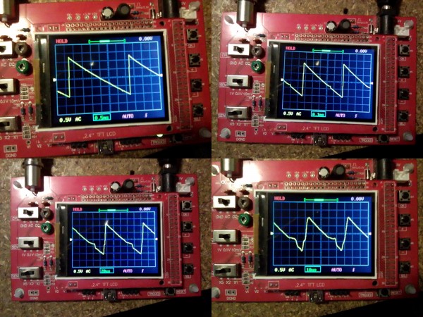
I have included the PDF files of the two saw cores. The images from the oscilloscope (it's a very, very cheap one) are from Pin 8 of U3.3 (TL074) in the Saw-Squ VCO.
The top left image is at 300Hz, top right is at 1.8kHz, bottom left is at 9kHz and bottom left is at 20kHz. In the top right image at 1.8kHz you can see a little bump appearing near the bottom of the downward slope which gets progressively worse as the frequency increases.
Does anyone know why this is happening and what can be done to improve the waveforms shape?
Any help would be greatly appreciated.
Thanks
NM
| Description: |
|
| Filesize: |
1.76 MB |
| Viewed: |
139 Time(s) |
| This image has been reduced to fit the page. Click on it to enlarge. |
|
| Description: |
|

Download (listen) |
| Filename: |
Schematic_NuttyMonk Saw-Squ VCO_2021-10-08.pdf |
| Filesize: |
145.25 KB |
| Downloaded: |
180 Time(s) |
| Description: |
|
Download (listen) |
| Filename: |
Schematic_NuttyMonk Saw-Core VCO1_2021-10-08.pdf |
| Filesize: |
99.69 KB |
| Downloaded: |
159 Time(s) |
|
|
|
Back to top
|
|
 |
kaputtpanzer

Joined: Nov 02, 2009
Posts: 139
Location: Cologne
Audio files: 15
|
| Posted: Sat Oct 09, 2021 4:13 am Post subject:
|
|
|
| I don't have an answer for you but maybe some ideas that could help you. At first I thought that it is some weird slew rate related Problem but the TL072 has a quite high slew rate. Though I don't think that this is causing your problem. I wonder if the bump in the saw wave is somehow related to the pulse width signal? Maybe there is some signal bleeding through into your saw output. Bleed through often becomes a problem at higher frequencies but usually this is more of a concern in microcontroller circuits operating in the mhz range. |
|
|
Back to top
|
|
|
kaputtpanzer
Joined: Nov 02, 2009
Posts: 139
Location: Cologne
Audio files: 15
|
| Posted: Sat Oct 09, 2021 4:19 am Post subject:
|
|
|
Looking at the pictures again I am somehow convinced that the bump is the falling edge of the PWM signal. That the wave form looks a bit "low pass filtered" at 20khz is caused by the slew rate limitation of the opamp. Usually audio vcos don't operate at those frequencies, this shouldn't be a problem tho. And finally it could also be that the dso138 is causing that bump  |
|
|
Back to top
|
|
|
NuttyMonk
Joined: Jun 30, 2020
Posts: 63
Location: UK
|
| Posted: Sat Oct 09, 2021 9:30 am Post subject:
|
|
|
Thanks for your suggestions kaputtpanzer.
At first i thought it might be the slew rate of the op-amp but when i checked the output of the CD40106 the distortion showed up there as well.
Then i thought it might be the oscilloscope so i turned up the sampling rate on my PC software to 96kHz and recorded the waveform there and got very similar results.
The only other thing i could think of was that both of the schematics use diodes as part of the oscillator core and wondered if that might be it.
I'll have to try something else. Probably going to complete a triangular core vco instead and see how that looks on the scope.
Thanks
NM |
|
|
Back to top
|
|
|
kaputtpanzer
Joined: Nov 02, 2009
Posts: 139
Location: Cologne
Audio files: 15
|
| Posted: Sat Oct 09, 2021 10:58 am Post subject:
|
|
|
| Well you could remove the diode to check if the problem still remains. You will end up with triangle wave if you remove it. |
|
|
Back to top
|
|
|
Buck Starchaser
Joined: Jan 13, 2022
Posts: 6
Location: USA
|
| Posted: Thu Jan 13, 2022 1:57 am Post subject:
Re: Why these distorted waveforms at higher frequency? |
|
|
In the second schematic, I believe C3 is part of the problem. The +12V power rail is feeding U1. U1 has a nominal output impedance of 125Ω. When U1.4 is fully on it will look like a 125Ω resistor from the +12V rail to its output, this forms a series loop that will translate to: C3+ in series with a 125Ω resistor, through diode D1, to C3-.
I believe this is why there is a bump at right about the voltage level that would smell like diode. Double-checking the time this anomaly takes, 5uS should be about one time constant, and it looks like about 2'ish TC's to settle on the highest frequency picture, and longer with the slower pictures. Diodes turn resistor-like right around their turn-on voltage, so that's likely causing the shelf component of the anomalies, as more time is spent in this resistive zone, and the logarithmic discharge curve of the capacitor meets the logarithmic resistive increase of the diode, followed by it cutting off completely for that rapid voltage drop, and the capacitor beginning to recharge for that little curve at the bottom.
I haven't spent enough time analyzing this circuit to make and test corrective edits. I just got here and this post caught my eye, so I made an account. I don't understand why C3 is connected like that, as it seems to only perform the function shown. If it is required for operation, then I would alter the deal and replace it with a very high-value resistor. Otherwise, I'd Widlarize that puppy.
The 1N4148 has a 4nS reverse recovery time, which is too fast for me to suspect D2 is causing the specific O-Scope images provided.
Hope this helps! |
|
|
Back to top
|
|
|
NuttyMonk
Joined: Jun 30, 2020
Posts: 63
Location: UK
|
| Posted: Thu Jan 13, 2022 5:12 am Post subject:
|
|
|
Since i posted this i went and bought a proper brand-new oscilloscope so i should go back and check it out again. I got the same problem on a VCO i built on a JLCPCB which i designed but i haven't gotten round to looking at it on the scope yet. I finally managed to get a job after over 10 years of unemployment so been a bit busy. Not as much time for electronics.
I'll try to test the new VCO on the scope and see if it looks the same as it did on the crappy scope. I had the feeling it might be the cheap scope which was the issue after seeing the same issue on a completely different circuit. It only happened on one particular setting of the crappy scope.
Will let everyone know the results when i get them.
Thanks for reminding me about this Buck.
Cheers
NM |
|
|
Back to top
|
|
|
Buck Starchaser
Joined: Jan 13, 2022
Posts: 6
Location: USA
|
| Posted: Thu Jan 13, 2022 2:42 pm Post subject:
|
|
|
I didn't really consider the "bad test equipment" angle, even though I built an O-Scope kit that looks identical to the one in the picture, tested it for a few minutes, and then hurled it into the abyss (meaning I pushed it farther into the pile of forlorn gadgetry).
If you didn't already have a replacement scope to compare, you could set up a simple resistor network to introduce a DC offset, if this particular scope design is having a problem around zero crossing. You could also place a decoupling cap on the circuit output to turn its output into an AC signal.
Congrats on your job! |
|
|
Back to top
|
|
|
PHOBoS

Joined: Jan 14, 2010
Posts: 5854
Location: Moon Base
Audio files: 709
|
|
|
Back to top
|
|
|
Buck Starchaser
Joined: Jan 13, 2022
Posts: 6
Location: USA
|
| Posted: Tue Jan 18, 2022 5:01 am Post subject:
|
|
|
| PHOBoS wrote: | I was just watching this video and the distortion you have looks awfully similar to the crossover distortion shown in it.
|
That was a good catch!
I did some research on the chip he used for that video (LM358), and found that it was designed to have a powerful mode, and an efficient mode, and that the distortion occurs when it doesn't stay in one mode (like when a capacitor is at peak current draw, ie. near zero crossing). Here is an excerpt from the paper.:
"To reduce the power supply current drain, the amplifiers have a class A output stage for small signal levels which
converts to class B in a large signal mode. This allows the amplifiers to both source and sink large output
currents. Therefore both NPN and PNP external current boost transistors can be used to extend the power
capability of the basic amplifiers. The output voltage needs to raise approximately 1 diode drop above ground to
bias the on-chip vertical PNP transistor for output current sinking applications.
For ac applications, where the load is capacitively coupled to the output of the amplifier, a resistor should be
used, from the output of the amplifier to ground to increase the class A bias current and prevent crossover
distortion. Where the load is directly coupled, as in dc applications, there is no crossover distortion" ~~ SNOSBT3I Rev.: Dec 2014 Texas Instruments
The circuit here seems to be using a TL074 though. Its datasheet does not make any statements about crossover distortion. |
|
|
Back to top
|
|
|
|

 Forum index » DIY Hardware and Software

