| Author |
Message |
Scott Stites
Janitor


Joined: Dec 23, 2005
Posts: 4127
Location: Mount Hope, KS USA
Audio files: 96
|
 Posted: Tue Dec 04, 2007 11:53 am Post subject: Posted: Tue Dec 04, 2007 11:53 am Post subject:
 Klee Sequencer Circuit Theory of Operation Klee Sequencer Circuit Theory of Operation
Subject description: An explanation of the circuits that comprise the electro-music Klee Sequencer |
  |
|
I thought it might be a good thing to begin compiling a circuit theory of operation here. When its complete, I'll compile it into a PDF. In the meantime, if you plan to read and study this, have a copy of your schematic handy. I'll start off with the Clock and Load functions, with Load being the first function described.
=============================
Load Function
U5, CD4013, performs the load function by controlling whether the shift register ICs are in the parallel or serial mode. For 99.99% of the time, the shift registers are in the serial mode.
In the serial mode, each shift register will cycle bits through the register, left to right. With each clock pulse, the bit present on the serial input of the shift register will enter the shift register, and the bit present in the eighth position of the shift register will pass out of the shift register.
In the parallel mode, each shift register will "look at" the bits programmed on its parallel inputs. The pattern switches set these bits. The switch to and from the parallel mode is a very fast operation - this mode looks at the bit pattern programmed by the pattern switches only long enough to load the data, then the shift registers revert back to serial mode.
While the shift registers are in the serial mode, they ignore the pattern that is programmed by the pattern switches.
Two shift register control signals are generated by U5. When the PSA signal goes high, it puts the shift registers in the serial mode. Immediately afterwards, the R Async signal goes high. When R Async goes high, it clocks the parallel data into the shift registers on its rising edge. Nearly as soon as it goes high, R Async goes low, which in turn causes PSA to go low, which puts the shift registers back in serial mode.
The CD4013 calls these shots, and it is told to do so by the rising edge of a pulse applied to the clock pin of its first stage (pin 3). There are three events that can produce this triggering event:
1. The Load Switch is pressed.
2. A pulse is produced by a signal applied to the external load input.
3. The Gate Bus 1 Load Switch is on, and Gate Bus 1 transistions to high.
Load Logic
In its initial state, U5 sections 1 and sections 2 will be in the "reset" condition - the "Q" signal of both sections will be low.
The rising edge of the signal applied to U5, pin 3, clocks the first section's Q signal (pin 1) high. This pulls the PSA signal high. When PSA is high, the two shift register ICs are put into the parallel mode.
When PSA ("Q" pin 1 of U5) transitions from low to high, the rising edge of this signal clocks the second stage of U5, because this signal is also connected to the clock input of the second section (pin 11).
Clocking the second section of U5 causes its Q signal to go high (pin 13). This creates a sharp rising pulse, which pulls the signal R Async high. The transition of R Async from low to high clocks the parallel data into the shift register ICs.
When R Async goes high (Q of the second section), this signal is squared up by R22/D3 and slightly delayed by C9. When it pulls high enough, this signal resets the second section of U5, because it is fed into the reset pin (pin 10).
Resetting the second section brings Q of the second section low, causing R Async to go low again. This transition also briefly pulls the voltage of pull-up resistor R20 low through C18. When this signal goes low, it causes the output of U2, Pin 8 to create a positive going pulse. This pulse is applied to the reset pin of the first section of U5 (pin 4), which pulls PSA low, placing the shift registers back into the serial mode. U5 is then ready to complete the operation again whenever the next load pulse is received.
Load Pulse Logic
Manual Load Switch: When the manual load switch is pressed, R27 is pulled low, which causes the voltage of R18 to pull low briefly through through C11, the "debounce" capacitor. When R27 is pulled low, it pulls pin 5 of U2 low, which causes pin 6 of U2 to snap high. This signal is ORed by U3 (pin 2) with any pulse that may be generated by the external load input, which would be present on pin 1 of U3. The output of this section of U3 is applied to pin 8 of U3, where it is ORed with any Gate Bus 1 signal that may be present on pin 9 of U3, and the signal is passed from pin 10 of U3 to the clock input of the first section of U5 (pin 3).
External Load Input: Signals applied to the external load input first pass through D1. D1 blocks any negative excursions present at the load input which prevents a negative excursion from potentially damaging U1. R21 acts as a load impedance and reference to ground for the incoming signal.
U1 acts as an input comparator. R25/R29 form a voltage divider which provides a voltage reference of around 1.96V for a 15V rail supply. This signal is applied to pin 2 of U1.
When the signal applied to pin 3 of U1 exceeds this reference voltage, it causes the output of U1 (pin 1) to rail high. Remember, the applied signal must first pass through D1, which drops its signal level by approximately 0.7V, so the input signal must exceed approximately 2.65V or so in order for the output of U1 to swing high. R92 adds hysteris to this input, so even a rounded input signal (such as a sine wave) will ensure a crisp "snap" to high from the output of U1.
The output of U1 is applied to pin 3 of U2, which causes pin 4 of U2 to snap low. The transition from high to low on pin 4 of U2 pulls the voltage of pull-up resistor R17 briefly low through C6. Pin 5 of U2 is thus drawn briefly low, causing pin 6 of U2 to pulse high.
This brief pulse is ORed by U3 (pin 1) with any pulse that may be generated by the manual load switch, which would be present on pin 2 of U3. The output of this section of U3 is applied to pin 8 of U3, where it is ORed with any Gate Bus 1 signal that may be present on pin 9 of U3, and the signal is passed from pin 10 of U3 to the clock input of the first section of U5 (pin 3).
Bus 1 Load Switch: When the Bus 1 Load switch is closed (Gate Bus 1 Load is set to "On"), the signal present on the internal Gate Bus 1 system is applied to pin 9 of U3. R26 provides a path to ground for pin 9 when the switch is open (Gate Bus 1 Load is set to "Off"). This signal is ORed with any pulse signals produced by the Load Switch and/or External Load input, which are applied to pin 8 of U3. When the output of U3 goes high, it clocks the first section of U5, because it is connected to the U5 clock input pin 3.
Pulse Logic Considerations: The Gate Bus 1 Load signal is the dominant control signal for clocking U5. Note that the signals produced by Load Switch and External Input are very quick pulses. They will rarely, if ever, coincide or interfere with each other. The Gate Bus 1 Load signal, however is derived directly from the internal gate bus 1 system. That means as long as any stage connected through a gate bus switch to Gate Bus 1 is active, this signal will be held constantly high until the shift registers step to a state where no active high stage is switched to gate bus 1, regardless of whether the clock is high or low. This means that, as long as the Gate Bus 1 signal is high, the clock input of U5 (pin 3) will be held high. As long as this pin is held high, no other signal can produce a low to high transition to initiate a pattern load. Therefore, while the Gate Bus 1 Load Switch is "On", and Gate Bus 1 is high, no load by either the load switch or the external load input will be possible.
_________________
My Site |
|
|
Back to top
|
|
 |
Scott Stites
Janitor
Joined: Dec 23, 2005
Posts: 4127
Location: Mount Hope, KS USA
Audio files: 96
|
| Posted: Mon Mar 24, 2008 8:39 pm Post subject:
|
|
|
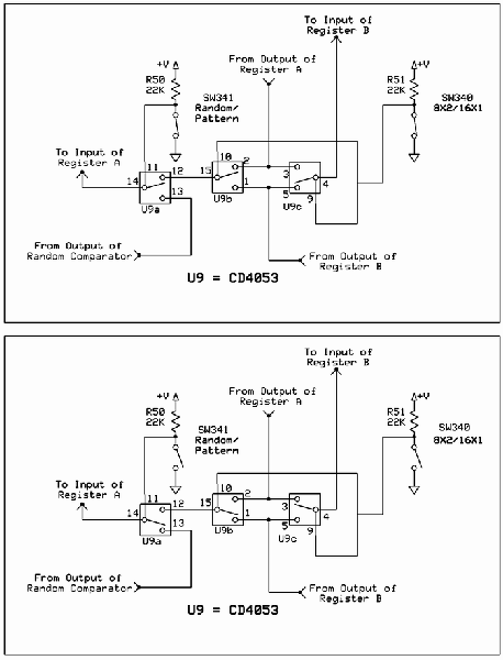
Klee Mode Switching
The Klee mode switch section consists of three controls:
1. The 8X2/16X1 Switch which determines if the two shift registers are linked together to form a single 16 bit register or two separate 8 bit registers.
2. The Random/Pattern Switch which determines if the input data to Shift Register A is recycled data from either Shift Register A or Shift Register B (depending on the setting of the 8X2/16X1 Switch) or instead is fed the data from the random input comparator.
3. The Invert B Switch which allows the output data of Register B to be inverted before it is recycled back to the input of either Register A, Register B, or neither (depending on the settings of the 8X2/16X1 Switch and/or the Random/Pattern Switch).
Two of the mode switches are SPST (Single Pole Single Throw) switches: the 8X2/16X1 Switch and the Random/Pattern Switch each switch a control voltage, either high or low, both of which are used to control U9, a CD4053, which is a Triple Two Channel Analog Multiplexer/Demultiplexer. The Invert B Switch is a SPDT (Single Pole Double Throw) switch that actually switches the output signal of Register B through or around a voltage inverter. The first section of this portion of the theory of operation will go into a bit more detail on the basic switching operation of the CD4053.
As mentioned before, U9 is a CD4053 Triple Two Channel Analog Multiplexer/Demultiplexer. That's a fairly intimidating name for what it actually is. Simply put, the CD4053 is an integrated circuit that consists of three SPDT switches. Each of these switches has a control pin; a low voltage on the control pin of a particular switch connects one "throw" pin to the "pole" pin, and a high voltage on the same control pin will connect the other "throw" pin to the "pole" pin. Like a mechanical switch, each of the switches on the CD4053 are bi-directional. In other words, the "throws" of a switch can act as either inputs or outputs and the "pole" pin can act as either an input or an output as well. Unlike a mechanical switch, in the standard configuration, which is used by the Klee, these IC switches can only pass positive voltages - negative voltages would destroy the IC. Fortunately, there is no chance that the 4053 will be exposed to negative voltages, unless, of course, the entire PCB has been wildly and sadly mis-wired during the build process. Certainly the IC can not be subjected to negative voltages through operation of the electro-music Klee Sequencer.
It may help to expand the illustration contained in this post as you read this.
Both control switches, SW341 (Random/Pattern) and SW340 (8X2/16X1) connect the positive rail to ground when closed, through R50 and R51 respectively. This has the effect of providing either a positive "high" or ground potential (low) to the three control pins of the CD4053. When each switch is closed, it provides the low to the pin to which it is connected. Refer to the top portion of the supplied illustration. Note that both switches are closed, so each is providing a low control signal. The Random/Pattern switch is connected to pin 11 of the CD4053, which controls switch represented by U9a. With the low signal, pin 12 is connected to pin 14, so any signal connected to pin 12 will pass to pin 14.
The 8X2/16X1 switch is actually connected to two control pins - pin 10, which is the control pin of the switch represented by U9b and pin 9, which is the control pin of the switch represented by U9c. In the top illustration, the 8X2/16X1 switch is in the closed position, so it is supply a low signal. This connects pin 2 to pin 15 and pin 4 to pin 5.
In the bottom portion of the illustration, each switch is open, which applies an active high to the control pins. Note now that U9a has pin 13 connected to pin 14, u9b has pin 1 connected to pin 15, and U9c has pin 4 connected to pin 3.
| Description: |
|
| Filesize: |
56.74 KB |
| Viewed: |
1544 Time(s) |
| This image has been reduced to fit the page. Click on it to enlarge. |
|
_________________
My Site |
|
|
Back to top
|
|
|
Scott Stites
Janitor
Joined: Dec 23, 2005
Posts: 4127
Location: Mount Hope, KS USA
Audio files: 96
|
| Posted: Mon Mar 24, 2008 10:06 pm Post subject:
|
|
|
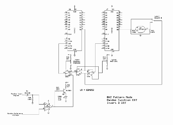
8X2/16X1 Pattern Function
The electro-music Klee Sequencer uses two 8 bit shift registers. In the 8X2 mode, the shift registers are configured to recirculate their own 8 bit patterns. In the 16X1 mode, the two shift registers are chained in series to form one 16 bit shift register. The 8X2/16X1 Pattern Switch determines whether the Klee operates as two 8 bit shift registers or one 16 bit shift register.
The 8X2 Pattern Mode
It may be of assistance to expand the Klee_encoder_8_2.png and refer to it as this section is read.
The illustration depicts the basic elements of the electro-music Klee Sequencer encoder section. The integrated circuits and components associated with the mode functions are shown with only the connections required to understand this section of the encoder displayed. U6 and U7 are CD4034 8 Stage Bidirectional Parallel/Serial Input/Output Bus Registers. U6 is Shift Register A, which handles the pattern bits for stages one through eight. U7 is Shift Register B, which controls the pattern bits for stages nine through sixteen. The actual logic and operation of the CD4034 is beyond the scope of this explanation, but suffice it to say they are each eight bit shift registers.
Pin 10 of the CD4034 is the input of the shift register. When a clock signal is applied to the CD4034, the value of the bit present at pin 10, high or low, is "fed into" the shift register. The output of each shift register is the eighth bit (pin 1). These are the only two data connections on the CD4034 that are concerned with the mode functions. Also shown are the positive rail connections and the ground connections for each CD4034.
A section of U4 (a CD4093 Quad 2-Input NAND Schmitt Trigger) is displayed on the output of Shift Register B (U7) - this is the inverter used in the Invert B function, which will be discussed later. Power connections to this IC are assumed in the illustration.
U8, which is one half of an LM358 Low Power Dual Operational Amplifier, and associated circuitry serves as the random function comparator. The operation of the random function will be discussed later as well.
Directly below U6 and U7 is U9, the CD4053 Mux IC, which is responsible for all of the switching required to facilitate the 8X2 and 16X1 functions. Its power connections (positive rail and ground) are assumed in this illustration.
In the 8X2 mode, Switch 340 (the 8X2/16X1 Mode Switch) is closed, which puts a low signal on control pins 9 and 10 of U9. This results in the direct connection between pin 2 and pin 15 and the direct connection of pin 4 and pin 5 of U9 pictured in the illustration. In this illustration, the signal path for each shift register can be traced. Lets begin with Shift Register A.
Lets assume Shift Register A contains data programed into it, either by the Pattern Switches or some previous random function operation. The data exits Shift Register A (U6) from pin 1. It travels to pin 2 of U9b. Though the data is also connected to pin 3 of U9c, U9c is configured to ignore that pin. However, U9b passes the signal to pin 15 of U9b, which is connected to pin 12 of U9a. U9a passes the signal from pin 12 to pin 14 of U9a. Pin 14 of U9a is connected to pin 10 of U6 (Shift Register A), thus a feedback loop is formed around Shift Register A. The signals travel through the shift register from input to output continuously.
Shift Register B is essentially the same story. Again, assuming Shift Register B (U7) has some data programmed into, we'll follow the path of the data. Data exits pin 1 of U7, and, because the Invert B function is turned off by the Invert B Switch (SW342), the data is connected directly to pin 5 of U9c. Notice that the data is also connected to pin 1 of U9b, but U9b is configured so that the "pole" of that section is not connected to pin 1. Instead, U9c passes the data present on pin 5 to pin 4 of U9c. Pin 4 of U9c is connected to pin 10 of U7, the data input of Register B, and thus, again, a feedback loop is formed around Register B.
The 16X1 Pattern Mode
Now take a look at the Klee_encoder_16_1.png illustration. Here we see that the 8X2/16X1 Switch (SW340) is open. This places a high signal on control pins 9 and 10 of U9, which alters the switching arrangement of U9b and U9c. Now our two 8 bit shift registers are joined together to form a single 16 bit shift register. Lets start at the output of Shift Register B (U7).
Again, we can assume at least one of the shift registers has some data to pass around. Invert B is off, so the output of U7 (pin 1) is connected directly to pin 1 of U9b, which is then routed to pin 15 of U9c. Pin 15 of U9c is connected to pin 12 of U9a, which is configured to pass that signal to pin 14 of U9a. Pin 14 of U9a is connected to the serial input of shift register A (U6), so now our data is passing directly out of Shift Register B (U7) to the input of Shift Register A (U6).
Our data passes through Shift Register A (U6) and is output at pin 1. Pin 1 of U6 is connected to pin 3 of U9c. U9c passes the data at pin 3 to pin 4 of U9c. Pin 4 of U9c is connected to pin 10 of U7 (Shift Register B), so now our data has made it full circle from the output of Shift Register B, through Shift Register A, and back to the input of Shift Register B again. Thus our two 8 bit shift registers are running in series forming a single 16 bit shift register. Our data will now pass through Shift Register B, back through Shift Register A, back through Shift Register B, and so on.
Note that this operation is predicated on the fact that the Random/Pattern Switch (SW341) remains closed. If the Random/Pattern Switch is opened, then the input to Shift Register A is dedicated to the output of the random comparator. This has implications on the operating modes of the electro-music Klee Sequencer that will be discussed in the next installment.
| Description: |
|
| Filesize: |
49.71 KB |
| Viewed: |
1758 Time(s) |
| This image has been reduced to fit the page. Click on it to enlarge. |
|
| Description: |
|
| Filesize: |
49.81 KB |
| Viewed: |
1610 Time(s) |
| This image has been reduced to fit the page. Click on it to enlarge. |

|
_________________
My Site |
|
|
Back to top
|
|
|
Scott Stites
Janitor
Joined: Dec 23, 2005
Posts: 4127
Location: Mount Hope, KS USA
Audio files: 96
|
| Posted: Tue Mar 25, 2008 10:51 am Post subject:
|
|
|
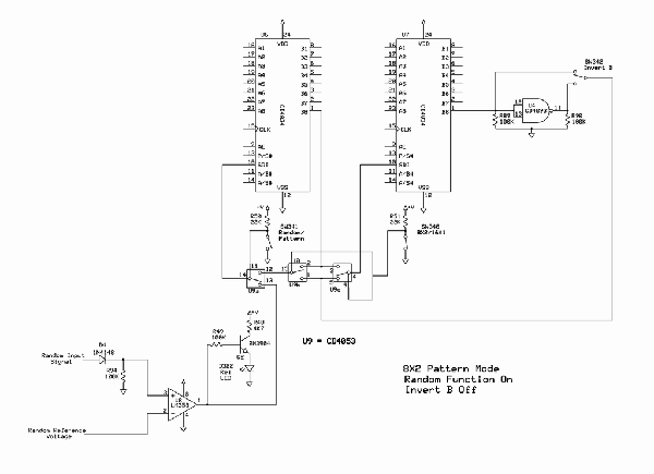
8X2/16X1 Random Function
The random function of the electro-music Klee Sequencer works by converting any signal applied to the random input into a series of high or low digital signals. This is done simply by comparing the positive portion of the random input signal to a reference voltage, and converting any portion of the input signal that exceeds the reference voltage to a "high" and any portion of the signal that falls below the reference to a "low".
When the Random/Pattern Switch is set to random operation mode, this series of high and low voltage levels is applied to the input of Shift Register A only. The 8X2/16X1 Switch will play a part in exactly how the random data is treated - whether it is limited to Shift Register A, or if the random data is passed through both shift registers.
Random 8X2 Operation
Refer to the illustration in Klee_Encoder_8_2_rand.png. In the illustration, we see that the 8X2/16X1 Switch (SW340) is closed, which puts the Klee into the 8X2 Mode. If you trace the signal from the output of Shift Register B, U7 pin 1, to the input of Shift Register B, U7 pin 10, you will see that Shift Register B will still recirculate its data.
However, the Random/Pattern Switch is now open - this pulls the control pin of U9a (pin 11) high, causing pin 12 to disconnect from pin 14 and causing pin 13 to connect to pin 14. This has the effect of connecting the output of U8, the random comparator, to the input pin of Shift Register A, U6, pin 10. This action also disconnects the output of Shift Register A, U6 pin 1, from the input of Shift Register A; Shift Register A will no longer recirculate its data. Any data bit sent to pin 10 will cycle through the register and "disapppear" at the output.
U8, the random comparator has two input signals. The front panel reference pot supplies a variable DC reference to pin 2 of U8. The signal applied to the Random Input Jack passes through the Random Level Pot, where the signal level can be attenuated before it is applied through D4 to pin 3 of U8. U8 is powered between the positive supply rail and ground, so D4 is supplied to block any potential negative voltage that is applied to pin 3. R94 acts as a reference to ground so pin 3 does not float.
U8 is configured as a simple comparator. If the signal applied to pin 3 has a greater voltage level than the reference voltage applied to pin 2, then the output at pin 1 will be a "high". If the signal applied to pin 3 has a lower voltage level than the reference voltage applied to pin 2, then the output at pin 1 will be a "low".
The signal present at pin 1 of U8 is applied to the base of Q2 through a 100K resistor. If pin 1 of U8 is high, Q2 conducts current, limited by R48, through the front panel Reference LED (D322), and the LED will illuminate. If pin 1 of U8 is low, no current will flow through D322, and it will remain dark. The output of U8 pin 1 is also now connected to the input of Shift Register A, U6 pin 10, through U9a.
As the voltage on pin 3 of U8 fluctuates above and below the reference voltage at pin 2, the output at pin 1 will produce a train of highs and lows. When Shift Register A is clocked and "looks at" its serial input, pin 10 of U6, the signal, high or low, will be shifted into the first cell of the shift register, which is the Stage 1 pattern bit. With each successive clock pulse, this bit will shift right, followed by other highs and lows generated by the random comparator.
In this configuration, because Shift Register B (U7) is still recirculating its data, stages 9 through 16 will continue to repeat a set pattern. Shift Register A is not recirculating its data, so the pattern bits that shift through it will vary constantly according to the nature of the signal applied to the Random Input Jack.
It should be noted that the sequence of bits originating from the random comparator could be considered random, pseudo-random, or even-random, depending on the nature of the signal applied to the random input. An analog noise source perhaps could be considered random; an LFO with a cycle frequency unrelated to the clock input could be considered pseudo-random, whereas a signal synchronized to the clock signal could be considered non-random. All three varients will have decidely different effect on the nature of the pattern passing through Shift Register A.
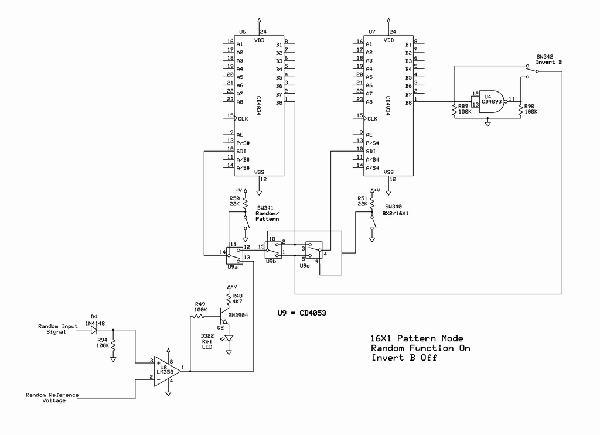
Random 16X1 Operation
Refer to the illustration in Klee_Encoder_16_1_rand.png. This illustration is essentially the same as the previous illustration, except now the 8X2/16X1 Switch is open, which applies a high level to U9 control pins 9 and 10, placing the Klee into the 16X1 mode.
Pattern 16X1 Mode differs from Random 16X1 mode in that the data within either of the shift registers cannot recirculate. The data generated by the random comparator instead is allowed to pass through both shift registers in a non-repeating fashion. Let's begin with the input of Shift Register A.
As an example, let's say at the point in time the clock signal driving the two shift registers rises to a high state while the output of U8, and thus the input to Shift Register A (U6, pin 10), is high. This high bit is loaded into the first cell of Shift Register A. As the clock cycles high and low, our bit travels through Shift Register A. At the end of eight clock pulses, the bit arrives at the output of Shift Register A (U6, pin 1). U6 pin 1 is now connected through U9c to the input of Shift Register B (U7, pin 10). On the next clock cycle, our bit enters Shift Register B. It travels through Shift Register B for eight clock cycles, whereupon it has arrived at the output of Shift Register B (U7, pin 1).
Now, follow the path of Shift Register B's output. First of all, Invert B is off, so it bypasses U4 - it's connected directly to pin 5 and pin 1 of U9. It cannot travel travel back to the input of Shift Register B (U7) because pin 5 of U9c is disconnected from pin 4 of U9c. It does, however connect to pin 15 of U9b, but can go no further. Pin 15 of U9b is connected to pin 12 of U9a, which is switched away from allowing the bit to travel back to Shift Register A - remember, Shift Register A is being fed by the random comparator. So, our bit, on the next clock cycle, just disappears - it has no way to recirculate.
The effect of this is that the random pattern can cycle across both shift registers, but it does not recirculate, so it has the potential to be ever-changing and non-repeating.
Next Installment: Invert B.
| Description: |
| Random 8X2 Function Diagram |
|
| Filesize: |
49.37 KB |
| Viewed: |
1379 Time(s) |
| This image has been reduced to fit the page. Click on it to enlarge. |
|
| Description: |
| Random 16X1 Function Diagram |
|
| Filesize: |
49.51 KB |
| Viewed: |
1413 Time(s) |
| This image has been reduced to fit the page. Click on it to enlarge. |
|
_________________
My Site |
|
|
Back to top
|
|
|
|

 Forum index » DIY Hardware and Software » Klee sequencer
