| Author |
Message |
handsfelloff
Joined: Sep 01, 2008
Posts: 24
Location: uk
|
 Posted: Mon Feb 23, 2009 6:41 am Post subject: Posted: Mon Feb 23, 2009 6:41 am Post subject:
 single vs double sided PCB layout would like advise single vs double sided PCB layout would like advise
Subject description: Need advise on a board layout I have made for tonner transfer method |
  |
|
Hi,
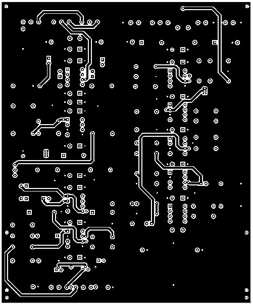
Heres a single sided design I made. I tried to create a pcb this weekend using toner transfer method. Unfortuantely after a number of attempts I had to admit defeat.
This design works, but only virtually. When it comes to ironing a transfer of the image the tracks merged and it was near imposible to dig the crud out of the tracks.
I was considering converting this to a double sided design then I could make the tracks and clearances wider.
The copper pour is the ground. One problem clearance between the tracks and the copper pour. In order to get the copper plane flowing around tracks and components I had to reduce the spacing to 10mil (0.010) that was too small for the toner transfer. I was wondering if I made a double sided should I make a copper pour on both the top and bottom layers then connect the pours with vias?
Any sagely advise would be very much appreciated in this pursuit of trail and error.
Thanks
Wilson
| Description: |
|
| Filesize: |
569.92 KB |
| Viewed: |
232 Time(s) |
| This image has been reduced to fit the page. Click on it to enlarge. |

|
| Description: |
|
| Filesize: |
591.01 KB |
| Viewed: |
209 Time(s) |
| This image has been reduced to fit the page. Click on it to enlarge. |

|
|
|
|
Back to top
|
|
 |
fonik

Joined: Jun 07, 2006
Posts: 3950
Location: Germany
Audio files: 23
|
| Posted: Mon Feb 23, 2009 7:02 pm Post subject:
|
|
|
i never did a homebrew double sided layout, so no comment on this from my side. however i did some single sided layouts and always tried to keep the tracks 40mil wide, at least 16mil. i never used ground planes and tried to keep the clearance above at least 24mil. worked fine using press and peel blue.
_________________

cheers,
matthias
____________
Big Boss at fonitronik
Tech Buddy at Random*Source |
|
|
Back to top
|
|
|
handsfelloff
Joined: Sep 01, 2008
Posts: 24
Location: uk
|
| Posted: Wed Feb 25, 2009 9:04 am Post subject:
|
|
|
Hey Fonik,
Thanks for your thoughts. Yeah I decided to keep give more space since this is a homebrew pcb job reduce the via's because thats a fiddle but maximise ground pours top and bottom stitching them together. Also decoupling power traces to ground to aid signal return paths over VCC and GND.
Heres my updated version. A bit chunkier as I used the top side for a few traces. Although I guess the wider the better for reducing induction and noise.
I think this may work better. It definately not the best, but its a start I will try this weekend. Happy times with the iron and acid 
| Description: |
|
| Filesize: |
529.93 KB |
| Viewed: |
209 Time(s) |
| This image has been reduced to fit the page. Click on it to enlarge. |

|
| Description: |
|
| Filesize: |
386.07 KB |
| Viewed: |
221 Time(s) |
| This image has been reduced to fit the page. Click on it to enlarge. |
|
| Description: |
|
| Filesize: |
599.42 KB |
| Viewed: |
210 Time(s) |
| This image has been reduced to fit the page. Click on it to enlarge. |

|
|
|
|
Back to top
|
|
|
etaoin

Joined: Jun 30, 2005
Posts: 761
Location: Utrecht, NL
|
Posted: Wed Feb 25, 2009 11:27 am Post subject:
Re: single vs double sided PCB layout would like advise
Subject description: Need advise on a board layout I have made for tonner transfer method |
|
|
| pushtin_cat wrote: | | I was wondering if I made a double sided should I make a copper pour on both the top and bottom layers then connect the pours with vias? |
I have made double sided boards at home and you generally want to avoid vias as much as you can. Metalized through holes are something you can't generally produce at home so you'll be soldering bits of wire through them all. In a new double sided home-etch design it's better to have both sides line up as much as possible at points that can be easily soldered on both sides, like resistor, diode or IC legs (if you don't use the cheap sockets).
_________________
http://www.casia.org/modular/ |
|
|
Back to top
|
|
|
fluxmonkey
Joined: Jun 24, 2005
Posts: 708
Location: cleve
|
| Posted: Wed Feb 25, 2009 1:08 pm Post subject:
|
|
|
i've heard of other folks doing doublesided boards with press-n-peel, but they're obviously more skilled than i am... my PNP layouts always seem to shift at least a little bit from where i initially position them. i'll stick to single sided.
i also have never tried anything with as extensive a groundplane as this... even w/ yusynth boards, i generally etch out all the copper that is not actual traces. for analog synth circuits (high levels, audio frequency) i've never had an issue.
what is this circuit?
b
_________________
www.fluxmonkey.com |
|
|
Back to top
|
|
|
fonik
Joined: Jun 07, 2006
Posts: 3950
Location: Germany
Audio files: 23
|
| Posted: Wed Feb 25, 2009 3:42 pm Post subject:
|
|
|
| bbob wrote: | | i also have never tried anything with as extensive a groundplane as this... |
and groundplanes without soldermask can spoil the party, when the clearance is small. it can cause you much trouble with shorts...
_________________
cheers,
matthias
____________
Big Boss at fonitronik
Tech Buddy at Random*Source |
|
|
Back to top
|
|
|
handsfelloff
Joined: Sep 01, 2008
Posts: 24
Location: uk
|
| Posted: Thu Feb 26, 2009 11:26 am Post subject:
|
|
|
| Good point fonik. Much more prone to short issues particulary with DIY tonner transfer method (http://myweb.cableone.net/wheedal/pcb.htm) thats why I have tried to allow for more generous clearances. The circuit is a pototype mishmosh of a polivoks filter(original soviet op amps) ms20 lfo and preamp to be bundled ito a kind of performance guitar/synth CV stompbox. Yeah bbob no timing sensitive circuitary here however these old opamps are sensitive and hopefully the idea of the substantial ground pour wil reduce noise and inductance. Although I havent tested this circuit yet (still got to sucessfully transfer...now im using argos catalog paper with a laminator to fuse the toner evenly so fingers x'd) ,but you are most likely right it probably does wont make a big difference with this kind of build. |
|
|
Back to top
|
|
|
fonik
Joined: Jun 07, 2006
Posts: 3950
Location: Germany
Audio files: 23
|
| Posted: Thu Feb 26, 2009 1:27 pm Post subject:
|
|
|
i used press'n'peel blue in the past with "mezzo mezzo" results. it worked fine for me, though:

_________________
cheers,
matthias
____________
Big Boss at fonitronik
Tech Buddy at Random*Source |
|
|
Back to top
|
|
|
handsfelloff
Joined: Sep 01, 2008
Posts: 24
Location: uk
|
| Posted: Tue Mar 03, 2009 8:52 am Post subject:
|
|
|
So I did manage to get an dbl sided etch out last saturday! Being super careful at each stage it took about 5 hours! I can honestly say the most problematic issue was clearances between the pour and the tracks also scrubbing off the paper (argos catalog brillant cheap paper)while being extra mindful not to scrub the toner off the board. I'll most likely design ground tracks for future diy boards. Still it would be a satisfying achivement to get this board to work.
Things I noticed after a few failours were that once I sanded with very fine wet/dry sand paper prior to transfer this created a good key for the toner to stick. I tried my laminator which probably works ok with less toner masking, but I ended up on the old iron. It takes practice...working how much pressure and heat to apply. Its tricky if you put too much is squashes the tracks...ug...patience but you get better. Now I just need to drill and hope to hell the top and bottoms matches without too much heat distortion error. I dont have much space (live on boat) so im buying a dremel with a PZ541 Vertical Drill Stand should be okay. |
|
|
Back to top
|
|
|
|

 Forum index » DIY Hardware and Software

