| Author |
Message |
warrenmaximus
Joined: Mar 10, 2012
Posts: 6
Location: St. Catharines, Ontario, Canada
|
 Posted: Sun Mar 11, 2012 4:03 pm Post subject:
Dual ADSR? Posted: Sun Mar 11, 2012 4:03 pm Post subject:
Dual ADSR?
Subject description: Ramblings about a modified TH ADSR Design |
  |
|
My thoughts are turning to ADSR modules as I near completion of my XR-VCO module (two parts on order to properly finish it off). I'm hoping nobody minds if I post a modified version of TH's ADSR design here. The schematic posted is my own, though the design is not completely original.
I've been thinking that I really want a Dual ADSR module in my rack, since you really want two- one for the VCA and one for the VCF.
But this got me to thinking, why duplicate the Gate/Trigger input circuits? For the ultimate in flexibility perhaps, but in my case I can't really imagine needing separately triggered ADSR modules.
So I decided to come up with a dual design, which shares one Gate input (I am not bothering with J1 "Trigger", as in TH's design).
I have some 2N7000 mosfets on hand, but not the CD4016/4066s that the original design used. So I modified the design to use these instead.
Somewhere else, I saw a design using a schmitt trigger for the gate input, so that it could be used with sloppy inputs. I am not totally happy with the hysteresis of my design yet, but it should provide about 0.4 volts worth.
I've attached the schematic and the LTspice simulation of it. Note that the first gate pulse is purposely sloppy to test the schmitt trigger action. You can see that it works.
(stuff about an added diode deleted -- I think I had simulation problems)
Update: I see a bunch of problems with this, so don't take this design to serious yet -- it's a work in progress.
Warren
| Description: |
| LTspice Schematic of the Dual ADSR |
|
| Filesize: |
50.51 KB |
| Viewed: |
658 Time(s) |
| This image has been reduced to fit the page. Click on it to enlarge. |

|
| Description: |
LTspice trace of the outputs of the Dual ADSR, using different settings for
each half unit. Note that the first gate pulse is purposely sloppy to test
the schmitt trigger action in Q1 & Q2. |
|
| Filesize: |
14.96 KB |
| Viewed: |
466 Time(s) |
| This image has been reduced to fit the page. Click on it to enlarge. |

|
|
|
|
Back to top
|
|
 |
warrenmaximus
Joined: Mar 10, 2012
Posts: 6
Location: St. Catharines, Ontario, Canada
|
Posted: Mon Mar 12, 2012 8:09 am Post subject:
Custom ADSR V2
Subject description: With ADSR Output Waveforms |
|
|
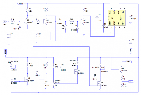
In this followup, I've just focused on a single ADSR unit. I did more testing and did indeed find that I needed D5 to keep the released wave form close to ground potential. I suspect that the poor off resistance of M3 was allowing some of the sustain voltage to leak back into C7 during the Release phase. Diode D5 makes sure that gets bled away by M4 to ground.
Another change that I made, was that I replaced the output TL071 buffer with a simple emitter follower. Since the low point of the C7 signal is near 0.6 volts, which isn't bad, but by using an emitter follower we can lower it to zero within a about a 100 mV or so. This also eliminates any need to feed -15V into the circuit, since it is all powered from the +15V rail.
The input Q3 and Q2 circuit has some improved hysteresis in this version as well.
The shown -15V supply need not be there. I have since removed it from the schematic.
The only puzzling thing I need to understand about this circuit, is why shortening the Release, ends up flattening out the sustain more. I don't understand the reason for that.
| Description: |
| The Attack pot is varied in this plot. |
|
| Filesize: |
10.54 KB |
| Viewed: |
7522 Time(s) |

|
| Description: |
| This schematic (with revisions) focuses on a single ADSR unit. To make it a dual, simply repeat the lower half of the schematic, and gang the outputs of Q3 and Q2 to the appropriate parts to trigger it in parallel with the first. |
|
| Filesize: |
57.52 KB |
| Viewed: |
492 Time(s) |
| This image has been reduced to fit the page. Click on it to enlarge. |
|
| Description: |
| In this plot, the Decay pot is stepped. |
|
| Filesize: |
13.59 KB |
| Viewed: |
486 Time(s) |
| This image has been reduced to fit the page. Click on it to enlarge. |

|
| Description: |
| The Sustain is stepped in this plot. |
|
| Filesize: |
15.55 KB |
| Viewed: |
469 Time(s) |
| This image has been reduced to fit the page. Click on it to enlarge. |

|
| Description: |
| The Release pot is stepped in this plot. |
|
| Filesize: |
12.95 KB |
| Viewed: |
455 Time(s) |
| This image has been reduced to fit the page. Click on it to enlarge. |

|
|
|
|
Back to top
|
|
|
warrenmaximus
Joined: Mar 10, 2012
Posts: 6
Location: St. Catharines, Ontario, Canada
|
Posted: Tue Mar 13, 2012 7:28 pm Post subject:
Custom ADSR V3
Subject description: Final Musings About Customized TH ADSR Circuit |
|
|
Those of you who bought Thomas Henry's book can compare their schematic to this one, if circuit design interests you. This will likely be my last post on this subject, unless discussion follows. Usually lack of discussion indicates yawns in the audience. 
I changed back to the TL071 buffer for the output in this design. I had failed to anticipate that the base of the emitter follower would have significant leakage to C7. I tried using another 2N7000 in a similar configuration, which more or less works. It however, it tends to have a more abrupt return to zero than the opamp (it needs a bit of head room). You could probably get away with it in an ADSR signal but I didn't like the idea of possibly hearing minor thumps at the tail end of a note.
I changed from using the TH diode logic to using a 2N3904 in Q5. Originally my Q4 was a 2N7000 fet, but I found that the turn off resistance was too low. This caused the release voltage to rise as high as 3 volts, when the decay was set near 90%. Sustain circuit current would leak and charge C7.
Replacing the fet with a bipolar solved the leakage problem. The bipolar Q4 does present a new problem in that when the sustain pot is set at 50%, the sustain level comes out to just over 3 volts (compare in the graphs below), instead of the more correct 2.5 volts. This is due to the 0.6 volt Vbe level where Q4 stops conducting and so cannot quite equalize the line to the established Sustain voltage.
Sustain at 50% for the TH design provides exactly 2.5 volts (at least in the LTspice simulation, using the CD4066). The CD4016 switches have low switching resistances of about 15 ohms. The CD4066 can get down to 10. In any case, these switches provide very low resistance and equalize to the Sustain voltage level nicely.
I've attached plot comparisons of my custom (V3) circuit compared to the published TH ADSR circuit. They seem to match closely, except for the Sustain level being higher for the same pot setting. The user can obviously compensate with the pot setting. The other area where I see a difference is in the spacings between equal changes in pot settings in the sustain step chart.
What does this exercise accomplish?
The CD4016/CD4066 is replaced primarily by discrete 2N7000 transistors. The CD4016 is actually the better design, if you have the parts.
The customized input gate circuit provides a bit of hysteresis, which allows sloppy audio signals to be used, if that is your thing. The TH design won't trigger if the gate signal is too slow in changing from low to high.
The bottom half of the schematic can be repeated to share the gate circuitry if you want a dual unit. It will of course also need it's own 555 timer chip.
I had fun working all this out in LTspice. Its far easier to try design changes in a simulation, with a click of the mouse. The only problem I ran into was that sometimes the simulation engine had trouble solving the simulation.
In the attached graphs below, the following ADSR pot settings are used, unless it is being stepped for that particular chart:
Attack is set to 90% (fast attack)
Decay is set to 90% (fast decay)
Sustain is set to 50% (level is half)
Release is set to 90% (fast release)
The stepped pot settings used are as follows:
5 % (low)
10%
25%
50%
75%
90%
95% (high)
Warren
| Description: |
| Where a parameter is varied, the pot settings used are: 5, 10, 25, 50, 75, 90, 95%. Where a pot is not varied, the following defaults apply: Attack, Decay and Release are set to 90% (fast). Sustain defaults to 50%. |
|
| Filesize: |
64.59 KB |
| Viewed: |
437 Time(s) |
| This image has been reduced to fit the page. Click on it to enlarge. |

|
| Description: |
|
| Filesize: |
53.75 KB |
| Viewed: |
512 Time(s) |
| This image has been reduced to fit the page. Click on it to enlarge. |

|
|
|
|
Back to top
|
|
|
|

 Forum index » DIY Hardware and Software » Thomas Henry designs
