| Author |
Message |
dk
Joined: Feb 12, 2019
Posts: 115
Location: Europe
|
|
|
Back to top
|
|
 |
PHOBoS

Joined: Jan 14, 2010
Posts: 5881
Location: Moon Base
Audio files: 709
|
 Posted: Fri May 21, 2021 7:34 am Post subject: Posted: Fri May 21, 2021 7:34 am Post subject:
|
  |
|
Ah I see what you are trying to do. Do you only have 3 spare inverters ?
I do see a way to do it with 4 but you could replace one with a transistor.
There might be another way so I'll think about it a little more.
If you don't need to control the data enable with a logic signal you could also just use a DPDT switch,
but that might introduce some unwanted bouncing.
_________________
"My perf, it's full of holes!"
http://phobos.000space.com/
SoundCloud BandCamp MixCloud Stickney Synthyards Captain Collider Twitch YouTube |
|
|
Back to top
|
|
|
dk
Joined: Feb 12, 2019
Posts: 115
Location: Europe
|
| Posted: Fri May 21, 2021 10:43 pm Post subject:
|
|
|
I have two of these behind the same panel, so I need to double whatever I do to them... I'm not at all against transistors, though (still smaller than adding an additional chip!).
| Quote: | If you don't need to control the data enable with a logic signal you could also just use a DPDT switch,
but that might introduce some unwanted bouncing. |
I considered that, but I've encountered problems with it, especially while the inputs are more or less directly wired up to the chip. Specifically, my existing 4031 modules completely clear their memory about 50% of the time I simply re-patch the clock, and I have a 4015 based module with switches (to share clock, shift the last bit of the first register to the second) that generally clears itself when I switch something. That may be a problem only with the clock inputs, but since I'm already taking it apart to modify it, I feel I might as well do it properly.
_________________
Horrors Of Dial-Up! on Facebook
Horrors Of Dial-Up! on Instagram |
|
|
Back to top
|
|
|
PHOBoS
Joined: Jan 14, 2010
Posts: 5881
Location: Moon Base
Audio files: 709
|
| Posted: Sat May 22, 2021 6:05 am Post subject:
|
|
|
Actually transistors wouldn't solve the problem which is that it ends up controling a diode AND with a diode OR and vice versa.
It can work but you have to pick the right resistor values. Also you are already using 1 inverter for debouncing so that just leaves 2 inverters.
I think it would be best to use those for the inputs, but if you just want to control the data enable with a switch and not a logic signal then that
frees up 1 inverter. Or just use an extra chip (wouldn't do it with a 4066 but use some boolean logic) might take up some extra space but so do
diodes/resistors/transistors.
_________________
"My perf, it's full of holes!"
http://phobos.000space.com/
SoundCloud BandCamp MixCloud Stickney Synthyards Captain Collider Twitch YouTube |
|
|
Back to top
|
|
|
dk
Joined: Feb 12, 2019
Posts: 115
Location: Europe
|
| Posted: Sat May 22, 2021 8:34 am Post subject:
|
|
|
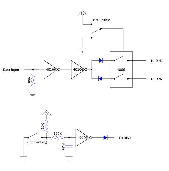
Do you think that the interaction between the diode AND and OR in the previously posted circuit wouldn't be covered by the output of the 40106? What would be the objection against using a switch like the 4066? I don't have enough panel space to both have a switch and be able to control the data enable with logic, so I'm going to stick with the switch.
Out of curiosity PHOBoS, how would you go about it?
Edit: I realize that working in simulation is hardly the same as it working in the real world, but at least it seems like it should work - https://tinyurl.com/yh9rg8eh
_________________
Horrors Of Dial-Up! on Facebook
Horrors Of Dial-Up! on Instagram |
|
|
Back to top
|
|
|
PHOBoS
Joined: Jan 14, 2010
Posts: 5881
Location: Moon Base
Audio files: 709
|
| Posted: Sat May 22, 2021 3:54 pm Post subject:
|
|
|
| dk wrote: | | Do you think that the interaction between the diode AND and OR in the previously posted circuit wouldn't be covered by the output of the 40106? |
if you put an inverter between them, then yes it will work fine but for this circuit to work there aren't enough inverters left.
| Quote: | | What would be the objection against using a switch like the 4066? |
It's a bit of a personal preference, when it comes to switching logic signals I like to use logic gates. This will provide a clean low
or high signal to work with, while something like a 4066 can result in a floating signal. Of course you can often add pullup or pulldown
resistors if needed.
| Quote: | | Edit: I realize that working in simulation is hardly the same as it working in the real world, but at least it seems like it should work - https://tinyurl.com/yh9rg8eh |
That circuit does not have the option to turn the data input off. Now you could simply add a single switch after the inverters
but try what happens if that switch would be open by removing one of the inverters and measure the voltages over the pullup
and pulldown resistors. You will see that those voltages are now closer to half the supply voltage and not really a usefull logic level.
The reason this happens is because the pullup and pulldown resistor are now basically configured as a voltage divider as a result
of the two diodes connected between them. You could test it though and see what it does.
If you want to use it with 2 switches of a 4066, which is probably your intention, then yes, that should work.
Keep in mind that if your data enable switch is bouncy the 4066 could still be bouncy aswell, but the signal is probably a bit cleaner than using just a switch.
_________________
"My perf, it's full of holes!"
http://phobos.000space.com/
SoundCloud BandCamp MixCloud Stickney Synthyards Captain Collider Twitch YouTube
Last edited by PHOBoS on Sat May 22, 2021 5:13 pm; edited 1 time in total |
|
|
Back to top
|
|
|
PHOBoS
Joined: Jan 14, 2010
Posts: 5881
Location: Moon Base
Audio files: 709
|
| Posted: Sat May 22, 2021 5:11 pm Post subject:
|
|
|
| Quote: | | Out of curiosity PHOBoS, how would you go about it? |
I was already preparing a bit for this. 
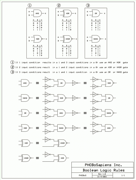
I attached a page with some 'rules' that are useful when designing a circuit like this, so have a look at that first.
You might want to keep it open in a seperate tab (or even print it out).
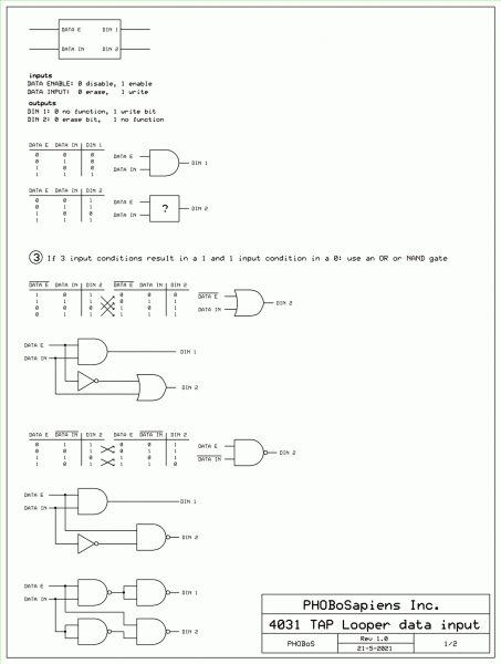
Here's one approach: (see 4031 TAP Looper data input 1a.gif)
First we have to figure out what to design, in other words what does it have to do ?
we'll need a circuit that has 2 inputs (DATA ENABLE, DATA IN) and 2 outputs (I labeled those DIN1 and DIN2 as that is what they will connect to)
note that these outputs connect to the DIN1 and DIN2 inputs using the diodes so that the write/erase switches can also be used.
- the function of the DATA ENABLE input is to disable [0] or enable [1] the data input.
- the function of the DATA INPUT is to erase [0] or write [1] a bit.
- DIN1 has to be [1] to write a bit, it doesn't do anything when it is [0] because of the diode in series with it.
- DIN2 has to be [0] to erase a bit, it doesn't do anything when it is [1] because of the diode in series with it.
with this information we can write down the truth tables for DIN1 and DIN2
| Code: | DATA E DATA IN | DIN1
-----------------|------
0 0 | 0
0 1 | 0
1 0 | 0
1 1 | 1
DATA E DATA IN | DIN2
-----------------|------
0 0 | 1
0 1 | 1
1 0 | 0
1 1 | 1 |
If we compare the truth table for DIN1 with the truth tables on the 'rules page' you'll see that this just requires an AND gate.
Of course you had already figured this out in 'tap-a-loop logic input complete.png' and it makes sense since you only want
DIN1 to be [1] when the data enable AND data input are both [1].
The truth table for DIN2 is not the same as one of the other standard gates but here we can make use of the 'rules' I labeled
(1) (2) (3). Since we need a gate for which 3 input conditions result in a [1] you can use an OR or a NAND gate. To this you only
have to invert one of the inputs. If you invert the DATA ENABLE input an OR gate can be used, if instead you invert the DATA INPUT
a NAND gate can be used.
The NAND gate is the most convenient option, because the circuit will then consist of an AND gate, an INVERTER and a NAND gate.
Both the AND gate and INVERTER can also be made with NAND gates (you can actually make any gate using NAND gates) which
results in a circuit that uses 4 NAND gates which you can get in a single package.
I have to admit that up to this point I kinda forgot that the reason you have the spare inverters is because you need 2 of them
for debouncing the write switch. So if you use NAND gates you'd still end up with 3 chips in total. But not all is lost which brings
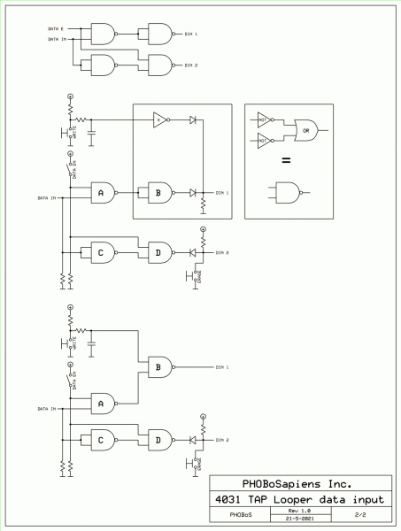
me to the next page (see 4031 TAP Looper data input 1b.gif)
I first drew up the complete schematic with the debounced write switch and erase switch. Now if we look at the circuit consisting
of the inverter(x), NAND(B) and the diode OR then what you have is just an OR gate with 2 inverted inputs. On the 'rules page'
you can see that the equivalent of that is just a NAND gate. So that part of the circuit can be replaced with a single NAND gate
which brings it back to a total of 4 NAND gates but now without the inverter and we got rid of 2 diodes and a resistor aswell.
Because there is a NAND gate available with schmitt trigger inputs (4093) the debouncing will still work. You could now even add
debouncing to the enable switch aswell if you want.
Of course with this circuit you'd still need 2 chips in total for 2 loopers.
| Description: |
|
| Filesize: |
79.69 KB |
| Viewed: |
364 Time(s) |
| This image has been reduced to fit the page. Click on it to enlarge. |
|
| Description: |
|
| Filesize: |
55.76 KB |
| Viewed: |
367 Time(s) |
| This image has been reduced to fit the page. Click on it to enlarge. |
|
| Description: |
|
| Filesize: |
48.82 KB |
| Viewed: |
376 Time(s) |
| This image has been reduced to fit the page. Click on it to enlarge. |
|
_________________
"My perf, it's full of holes!"
http://phobos.000space.com/
SoundCloud BandCamp MixCloud Stickney Synthyards Captain Collider Twitch YouTube
Last edited by PHOBoS on Wed May 26, 2021 10:17 am; edited 1 time in total |
|
|
Back to top
|
|
|
dk
Joined: Feb 12, 2019
Posts: 115
Location: Europe
|
| Posted: Wed May 26, 2021 1:23 am Post subject:
|
|
|
Sorry for not answering immediately... I'm still digesting everything!
I'm super grateful for you post PHOBoS. You could have just as easily only thrown a schemo up and not explained anything, but you've even explained how you came up with it. It makes for a much better learning experience, which is awesome.
On to the material itself:
| Quote: | | If you want to use it with 2 switches of a 4066, which is probably your intention, then yes, that should work. |
Yes, that was my intention, and it's why I didn't bother to put the data enable switch in the simulation. I had thought you meant there would be a problem when the circuit was connected. Your approach with logic gates looks a bit more elegant, though, so I'll need to pick up some 4093's 
In thinking about the de-bouncing thing, though, I was wondering how much of a problem has to do with the switch making contact vs other factors, namely ESD. I haven't been using protection resistors on inputs so I experimented with adding them to the 4031 module. If I re-patch the clock cable while maintaining contact (with my hand), it doesn't glitch. If I'm not touching the synth, though, and just re-patch, I lose at least some (if not all) of the data stored in the register. I'm wondering if this same thing can happen while flipping a toggle switch? If so, do you think the resistor between the switch and the schmitt trigger would be enough to prevent this from happening?
_________________
Horrors Of Dial-Up! on Facebook
Horrors Of Dial-Up! on Instagram |
|
|
Back to top
|
|
|
PHOBoS
Joined: Jan 14, 2010
Posts: 5881
Location: Moon Base
Audio files: 709
|
| Posted: Wed May 26, 2021 11:45 am Post subject:
|
|
|
| dk wrote: | Sorry for not answering immediately... I'm still digesting everything!
I'm super grateful for you post PHOBoS. You could have just as easily only thrown a schemo up and not explained anything, but you've even explained how you came up with it. It makes for a much better learning experience, which is awesome. |
Take your time and if you have any questions just ask. And yeah I could have just posted a schematic but it's the teach-a-man-to-fsh thing,
so if you learn anything from it then that's awesome indeed!
| Quote: | | If I re-patch the clock cable while maintaining contact (with my hand), it doesn't glitch. If I'm not touching the synth, though, and just re-patch, I lose at least some (if not all) of the data stored in the register. I'm wondering if this same thing can happen while flipping a toggle switch? If so, do you think the resistor between the switch and the schmitt trigger would be enough to prevent this from happening? |
interesting. if you patch it to a signal that is low it shouldn't do anything, but if that signal is high then you will create a series of low-to-high pulses.
Not sure why that would erase anything though, at least not when setup as a looper. Maybe the pulses are too fast or too noisy and the chip gets
a bit confused. You could try a resistor in series and a very small capacitor to GND to function as a low pass filter. That would also slightly delay the signal
but not in an audible way. However, if you combine the circuit with other circuits that use the same clock signal you might run into some issues.
Note that as far as I am aware it doesn't have a schmitt trigger on the clock input so the cutoff frequency would still have to be very high
but you can experiment to see if it helps. I don't think just a resistor would have much of an effect (apart from protection) but give it a try.
Another thing, data is only read on a low-to-high clock signal so any bouncing on the write/erase lines shouldn't have an effect on the shiftregister
unless your clock speed is even higher than the bounce frequency. Of course if the clock transition happens just while it's bouncing than it might
not read the value you want. It's also wired directly to the outputs using the NOR gates so you still get the bouncing there anyway.
_________________
"My perf, it's full of holes!"
http://phobos.000space.com/
SoundCloud BandCamp MixCloud Stickney Synthyards Captain Collider Twitch YouTube |
|
|
Back to top
|
|
|
elgabrielcichero
Joined: May 01, 2020
Posts: 2
Location: buenos aires
|
| Posted: Wed Mar 08, 2023 4:32 pm Post subject:
4031 TAP LOOPER DELUXE |
|
|
Dear All:
I tried the Shift Register 4031 Tap Looper.
It works fine, in my testing i found that after the 64 bit cycle, the gates recorded are "shifted one bit down" in relation to the main clock / data recorded.
I did a "musical" test, using a 8 step sequencer feeding the seq and the tap looper with the same clock source and taping on this pulses number:
1,9,17,25,33,41....
after the cycle, its play:
8,16,24, etc...
I thought that maybe, inverting the clock input could do the trick.
Any ideas?
Thanks! |
|
|
Back to top
|
|
|
PHOBoS
Joined: Jan 14, 2010
Posts: 5881
Location: Moon Base
Audio files: 709
|
| Posted: Tue Mar 14, 2023 11:39 am Post subject:
|
|
|
my brain isn't really cooperating with me right now but if you are manually tapping it might just be a timing issue.
If you want to "store" step 9 you will have to hold the button during the clk when it transitions from step 9 to 10.
If you try to do it exactly at the start of step 9 it could be that you are simply too early.
If you are feeding it data remotely then all kinds of things could happen if the data pin toggles at the same moment as the clk pin.
I'd say it's also not really how this circuit is intended. It functions best when running at a higher speed and for storing short sequences.
for example you could have it run along an 8 step sequencer at a frequency that is 8x the sequencers' clk speed.
_________________
"My perf, it's full of holes!"
http://phobos.000space.com/
SoundCloud BandCamp MixCloud Stickney Synthyards Captain Collider Twitch YouTube |
|
|
Back to top
|
|
|
|

 Forum index » DIY Hardware and Software » Lunettas - circuits inspired by Stanley Lunetta