| interested in a PCB or 4? |
| yep |
|
98% |
[ 151 ] |
| nope |
|
1% |
[ 2 ] |
|
| Total Votes : 153 |
|
| Author |
Message |
KEYKEYEYEKIT

Joined: Sep 08, 2009
Posts: 24
Location: Atlanta
|
 Posted: Sat Jul 10, 2010 8:28 pm Post subject:
Excited. Posted: Sat Jul 10, 2010 8:28 pm Post subject:
Excited. |
  |
|
| Hi, I'd be in for 2 boards when the new ones are ready to go. Thanks! |
|
|
Back to top
|
|
 |
ChrisCoady
Joined: Feb 27, 2010
Posts: 8
Location: NYC
|
| Posted: Sun Jul 11, 2010 10:16 am Post subject:
|
|
|
| is this still happening? if so i'll take multiple boards. |
|
|
Back to top
|
|
|
scriptstyle

Joined: Jan 22, 2008
Posts: 250
Location: nj
|
| Posted: Tue Jul 13, 2010 10:58 am Post subject:
|
|
|
| YESSSS. finally had some spare time and finished a pair of these! so much fun to play with thanks Topp(the 10 mins i had) i am still to add the both mod, and i am unsure how to separate the the gate priority from trigger. |
|
|
Back to top
|
|
|
ricoloverde
Joined: Nov 09, 2009
Posts: 39
Location: berkeley
|
| Posted: Mon Sep 20, 2010 5:21 pm Post subject:
281 CLONE PROJECT |
|
|
edit: found
Hey does anyone happen to have 2 spare 281 boards...
will there be another run anytime soon?
thanx
rico |
|
|
Back to top
|
|
|
equalpyramid
Joined: Oct 09, 2010
Posts: 5
Location: Canada
|
| Posted: Mon Oct 11, 2010 4:24 pm Post subject:
|
|
|
Yes, please make more of these. I'll take a couple.  |
|
|
Back to top
|
|
|
zthee

Joined: Feb 20, 2008
Posts: 414
Location: Stockholm
|
|
|
Back to top
|
|
|
LektroiD

Joined: Aug 23, 2008
Posts: 1019
Location: Scottish Borders
Audio files: 2
G2 patch files: 2
|
| Posted: Sun Nov 14, 2010 2:55 pm Post subject:
|
|
|
I'm a bit confused by the phrasing here, as I want to build a 12V version of the board.
| Quote: | | R7,R8: FOR 12V OPERATION USE 1.2/1.5K HERE |
Does this mean use a 1.2K for R7, and a 1.5K for R8,
or
use either value for both, ie R7,R8 = 1.2K (or 1.5K)?
_________________
LektroiD |
|
|
Back to top
|
|
|
toppobrillo

Joined: Dec 10, 2005
Posts: 766
Location: oakland, ca
G2 patch files: 1
|
| Posted: Mon Nov 15, 2010 4:38 am Post subject:
|
|
|
| Quote: | Does this mean use a 1.2K for R7, and a 1.5K for R8,
or
use either value for both, ie R7,R8 = 1.2K (or 1.5K)? |
the latter |
|
|
Back to top
|
|
|
LektroiD
Joined: Aug 23, 2008
Posts: 1019
Location: Scottish Borders
Audio files: 2
G2 patch files: 2
|
| Posted: Wed Nov 17, 2010 2:54 pm Post subject:
|
|
|
I couldn't find any L7810, I could only get TS7810CZ.. Are these ok?
Also, I have HEF4001BP, are these good substitutes for CD4001B?
_________________
LektroiD |
|
|
Back to top
|
|
|
toppobrillo
Joined: Dec 10, 2005
Posts: 766
Location: oakland, ca
G2 patch files: 1
|
| Posted: Wed Nov 17, 2010 11:55 pm Post subject:
|
|
|
| Quote: | I couldn't find any L7810, I could only get TS7810CZ.. Are these ok?
Also, I have HEF4001BP, are these good substitutes for CD4001B? |
yep, sounds good! the L7810 is just a generic name, LM_ i think is National Semi or whatever. TS i guess is just the mfr.s name. |
|
|
Back to top
|
|
|
LektroiD
Joined: Aug 23, 2008
Posts: 1019
Location: Scottish Borders
Audio files: 2
G2 patch files: 2
|
| Posted: Sun Nov 21, 2010 10:05 pm Post subject:
|
|
|
Ok, I've decided to go with this design, since it would look best in my system, I have the panels drilled and ready (image below text)..
I have carefully followed all the wiring diagrams in the documentation, but it seems there is a lot missing, so I am now at a brick wall. I do not know what to wire up where, it is really confusing me, hopefully someone could simplify it.
Basically there is a PK IN and PK OUT on the panel, but only a PKO on the board. First off I have never heard of PK OUT or PK IN on any other module, what does this mean, what do they do, and why is there no place to wire PK IN on the board?
Next, there's a CV1 and CV2 on the board, although the panel only has knobs for CV (presumably for CV1?), do I wire CV1 from board A to one CV pot on the panel, and CV1 from board B to the other, or do these connect only to one board?
Also confused about the 'END' sockets on the panel there is no END point on the PCB to wire these to?
Then there's the PI OD wiring points on the PCB, what are these for?
And how do I connect the Attack & Decay sockets?
a simple 'Go look at the schematic' response will mean these boards will remain in my box with the rest of my unfinished projects until the end of time, as schematics are not my strong point. I can relate better to drawn out wiring diagrams; would someone please be kind enough to draw out a wiring diagram of how it is supposed to be, maybe with an explanation of the above, as that seems to be missing from the documentation.

_________________
LektroiD |
|
|
Back to top
|
|
|
toppobrillo
Joined: Dec 10, 2005
Posts: 766
Location: oakland, ca
G2 patch files: 1
|
| Posted: Mon Nov 22, 2010 2:59 am Post subject:
|
|
|
| Quote: | Ok, I've decided to go with this design, since it would look best in my system, I have the panels drilled and ready (image below text)..
I have carefully followed all the wiring diagrams in the documentation, but it seems there is a lot missing, so I am now at a brick wall. I do not know what to wire up where, it is really confusing me, hopefully someone could simplify it.
Basically there is a PK IN and PK OUT on the panel, but only a PKO on the board.
|
"PI" is 'peak in'
| Quote: | | First off I have never heard of PK OUT or PK IN on any other module, what does this mean, what do they do, and why is there no place to wire PK IN on the board? |
see above- it is an analog "OR" function- the output "po" will be the maximum value at any of the circuit's 2 [or 3 if you added the xternal peak input] ins..
| Quote: | | Next, there's a CV1 and CV2 on the board, although the panel only has knobs for CV (presumably for CV1?), do I wire CV1 from board A to one CV pot on the panel, and CV1 from board B to the other, or do these connect only to one board? |
who's panel design was this? it doesn't really make sense, I would assume it was for a "both" CV input, but then I do not see the jack ? so- no idea. the 281 has 2 CV ins, 1 for att and 1 for dec. the original doesn't have input attenuators for these.
| Quote: | | Also confused about the 'END' sockets on the panel there is no END point on the PCB to wire these to? |
the end pulse is available at the "pls" pad on the PCB.
| Quote: | | Then there's the PI OD wiring points on the PCB, what are these for? |
I think you must mean PI and PO. PI is peak in and PO is peak out.
| Quote: | | And how do I connect the Attack & Decay sockets? |
they would go to the CV1 and CV2 pads.
| Quote: | a simple 'Go look at the schematic' response will mean these boards will remain in my box with the rest of my unfinished projects until the end of time, as schematics are not my strong point. I can relate better to drawn out wiring diagrams; would someone please be kind enough to draw out a wiring diagram of how it is supposed to be, maybe with an explanation of the above, as that seems to be missing from the documentation.
|
sorry- I didn't do the best job with this and admittedly the nomenclature of the boards is a bit weird.. I hope this helps though and please ask more questions if you have them! |
|
|
Back to top
|
|
|
LektroiD
Joined: Aug 23, 2008
Posts: 1019
Location: Scottish Borders
Audio files: 2
G2 patch files: 2
|
| Posted: Mon Nov 22, 2010 7:26 am Post subject:
|
|
|
Hi topp, thanks for your reply, just need to clarify a couple of details before attacking this with my soldering iron
| topp wrote: | | Quote: | Basically there is a PK IN and PK OUT on the panel, but only a PKO on the board.
|
"PI" is 'peak in'
| Quote: | | First off I have never heard of PK OUT or PK IN on any other module, what does this mean, what do they do, and why is there no place to wire PK IN on the board? |
see above- it is an analog "OR" function- the output "po" will be the maximum value at any of the circuit's 2 [or 3 if you added the xternal peak input] ins.. |
Is it best to wire these from board A or B?
Also what is the pad labelled 'PKO' for on the boards if 'PO' is already Peak Out?
_________________
LektroiD |
|
|
Back to top
|
|
|
toppobrillo
Joined: Dec 10, 2005
Posts: 766
Location: oakland, ca
G2 patch files: 1
|
| Posted: Mon Nov 22, 2010 8:47 am Post subject:
|
|
|
| Quote: | Is it best to wire these from board A or B?
Also what is the pad labelled 'PKO' for on the boards if 'PO' is already Peak Out? |
either, it really doesnt matter which. once you start to look at the pads VS how your panel components are situated, it will probably make more sense to do one or the other.
the PKO simply bypasses the 1K output series resistor [that gets wired to your OUT jack] and , following the "A vs B" board" document, u see the way it's used depends on the board configuration .
http://www.sdiy.org/toppobrillo/DOWNLOADS/2814_V3/SCHEME%20B%20BOARD%20v3.pdf
see the bottom left- PKO from "A" board goes straight to "PI", and PKO from "B" board goes to the pot.
does it make sense? |
|
|
Back to top
|
|
|
LektroiD
Joined: Aug 23, 2008
Posts: 1019
Location: Scottish Borders
Audio files: 2
G2 patch files: 2
|
|
|
Back to top
|
|
|
LektroiD
Joined: Aug 23, 2008
Posts: 1019
Location: Scottish Borders
Audio files: 2
G2 patch files: 2
|
| Posted: Fri Nov 26, 2010 1:04 am Post subject:
|
|
|
Still trying to work this out...
Has anyone completed this could maybe help me out here? A simple 'yes that works', or 'no it's not right' would be great..
I have the panel sat in my system, and the boards waiting, everything so far is wired as to the documents, just waiting for the missing wiring diagrams...
Please can someone help here, there must be at least one person who's completed this.
_________________
LektroiD |
|
|
Back to top
|
|
|
LektroiD
Joined: Aug 23, 2008
Posts: 1019
Location: Scottish Borders
Audio files: 2
G2 patch files: 2
|
| Posted: Fri Nov 26, 2010 7:09 am Post subject:
|
|
|
Nobody?
Maybe I should just sell these 4 boards (populated but not wired) and just buy the new versions.. Otherwise they will just sit in my box for the rest of eternity, no good to me there.
What's the value as they stand?
_________________
LektroiD |
|
|
Back to top
|
|
|
The Bad Producer

Joined: Mar 08, 2009
Posts: 282
Location: The Manhole
|
| Posted: Fri Nov 26, 2010 11:36 am Post subject:
|
|
|
Hey Lektroid, I can help you out with this, I could do a wiring doc maybe? But unfortunately not tonight, I could try and get something up tomorrow?
Charlie
_________________
http://loudestwarning.tumblr.com/ |
|
|
Back to top
|
|
|
LektroiD
Joined: Aug 23, 2008
Posts: 1019
Location: Scottish Borders
Audio files: 2
G2 patch files: 2
|
| Posted: Fri Nov 26, 2010 12:12 pm Post subject:
|
|
|
Thank you! That would be brilliant.. I presume my wiring was not right after all..
Much appreciated, I look forward to it.
_________________
LektroiD |
|
|
Back to top
|
|
|
toppobrillo
Joined: Dec 10, 2005
Posts: 766
Location: oakland, ca
G2 patch files: 1
|
| Posted: Fri Nov 26, 2010 8:38 pm Post subject:
|
|
|
| hi lektroid- sorry for my late reply! i had a look, it looks OK to me- except you'll have to add a series diode inline w the peak in jack. other than that, i think ur good to go.. |
|
|
Back to top
|
|
|
LektroiD
Joined: Aug 23, 2008
Posts: 1019
Location: Scottish Borders
Audio files: 2
G2 patch files: 2
|
| Posted: Sat Nov 27, 2010 12:03 pm Post subject:
|
|
|
Thanks topp, I'll probably hold off wiring anything until Charlie posts a wiring diagram, just to double make sure I'm doing everything right
For example I'm not quite sure what you mean by the series diode, or which direction it goes. Or how I'm going to stuff 2 pieces of wire into the PI pad on the A board without making the hole on the PCB bigger etc.
_________________
LektroiD |
|
|
Back to top
|
|
|
LektroiD
Joined: Aug 23, 2008
Posts: 1019
Location: Scottish Borders
Audio files: 2
G2 patch files: 2
|
| Posted: Tue Nov 30, 2010 3:32 am Post subject:
|
|
|
Board B doesn't work.. 
I have some voltage through it, but doesn't seem to be powered properly. For example, I tested the voltage at the voltage regulator on both boards (although only the "A" board has the regulator & 47µF cap in place).
On board "A" I get 10V at both outer pins of the regulator, and nothing at the centre pin. Board "B" I only get voltage at one of the outer pins.
Board "A" I get around 11V at pin3 of the pots; on board "B", I get nothing on either.
I wired the 10V pad on board "A" to the 10V pad of board "B", and also grounded both boards - I would assume this would be enough to power the boards?
I still haven't wired the Peak In jack, as I've not had confirmation of what is meant by series diode, or the orientation.
Maybe I jumped the gun and should have waited for The Bad Producer's full wiring diagram before diving into this, but I've held off for long enough and just want it built now
I hope someone can help (maybe double check the diagram I posted too)..
_________________
LektroiD |
|
|
Back to top
|
|
|
The Bad Producer
Joined: Mar 08, 2009
Posts: 282
Location: The Manhole
|
| Posted: Tue Nov 30, 2010 3:38 am Post subject:
|
|
|
Hi Lektroid,
Sorry life swallowing me up, but I'll be around tonight, should be able to upload stuff, I need to get mine out and make a few changes to the panel, so I can try and get a wiring doc up and maybe do some comparative tests etc...
Charlie
PS what sort of Volt reg did you use, 78L10?
Edit, I'll also have the wiring doc, just wondering how you did the panel, I had A and B both going through pots to the PEAK circuitand an external input... here is my front panel design...

_________________
http://loudestwarning.tumblr.com/ |
|
|
Back to top
|
|
|
LektroiD
Joined: Aug 23, 2008
Posts: 1019
Location: Scottish Borders
Audio files: 2
G2 patch files: 2
|
| Posted: Tue Nov 30, 2010 11:03 am Post subject:
|
|
|
| The Bad Producer wrote: | Hi Lektroid,
Sorry life swallowing me up, but I'll be around tonight, should be able to upload stuff, I need to get mine out and make a few changes to the panel, so I can try and get a wiring doc up and maybe do some comparative tests etc...
Charlie
PS what sort of Volt reg did you use, 78L10?
Edit, I'll also have the wiring doc, just wondering how you did the panel, I had A and B both going through pots to the PEAK circuitand an external input... here is my front panel design...
|
Hi, I used a 7810 regulator for mine, as suggested in the build docs.
The peak wiring is as above, with the cathode of the 4148 splitting off to both PI and PKO on the "A" board (I was not aware there is another way to do this).
I found a 5U design in the first few pages of this thread, and chose this one (although I did not add the CV pots).
http://electro-music.com/forum/phpbb-files/buchla2_164.jpg
Comparison tests sound good.. I wonder, do you have Skype or something similar so we can do them in realtime?
_________________
LektroiD |
|
|
Back to top
|
|
|
The Bad Producer
Joined: Mar 08, 2009
Posts: 282
Location: The Manhole
|
| Posted: Tue Nov 30, 2010 12:10 pm Post subject:
|
|
|
no skype but u can pm?
what board is your peak circuit on?
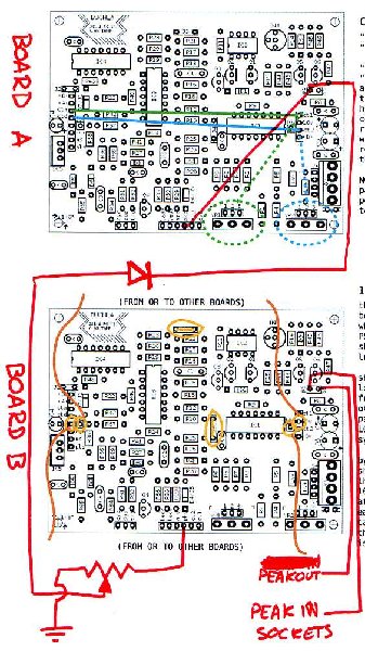
edit: your diagram looks wrong for one reason, I should have noticed this earlier... the PEAK circuitry is only built on one board - think of it as a separate sub-circuit - so the PEAK IN socket should go to the same PI pad as A PKO and B PKO, the output of this sub-circuit is PO.
edit edit: just working on a diagram
edit edit edit - you know you need to supply +15v, GND and -15V to each board? (sorry!)
_________________
http://loudestwarning.tumblr.com/ |
|
|
Back to top
|
|
|
|

 Forum index » DIY Hardware and Software