| Author |
Message |
cerkit

Joined: Nov 17, 2016
Posts: 17
Location: Montgomery, AL USA
|
 Posted: Sat Dec 10, 2016 10:04 am Post subject:
Clock signals through a Transistor Posted: Sat Dec 10, 2016 10:04 am Post subject:
Clock signals through a Transistor
Subject description: Is this possible? |
  |
|
Consider a scenario:
* Microcontroller (Raspberry Pi in this case)
* Oscillator output (in this case it's just a simple 40106 single oscillator)
* Transistor
* Trigger signal (from GPIO pins of Raspberry Pi)
I'd like to be able to send the signal of the oscillator through the transistor so it can be triggered by the microcontroller.
Is this possible or do I need to look at it differently?
Will this have an impact on the oscillator (something tells me the transistor will alter the signal in some way).
If not a transistor, what's the best way to gate the output of an oscillator?
Should I use the transistor between the "loop" resistor on the oscillator and the output pin?
Maybe between the capacitor to ground and the "input" pin of the oscillator?
Thanks in advance for any insight. |
|
|
Back to top
|
|
 |
PHOBoS

Joined: Jan 14, 2010
Posts: 5818
Location: Moon Base
Audio files: 709
|
| Posted: Sat Dec 10, 2016 10:40 am Post subject:
|
|
|
yes a transistor can work, downside is that the output wil be floating when turned off so you might need an extra pulldown resistor. Better would
be to use an AND gate since you are using digital signals, or probably even better: make the oscillator using a schmitt trigger NAND gate (CD4093).
You can find an example of those here
_________________
"My perf, it's full of holes!"
http://phobos.000space.com/
SoundCloud BandCamp MixCloud Stickney Synthyards Captain Collider Twitch YouTube |
|
|
Back to top
|
|
|
wackelpeter
Joined: May 05, 2013
Posts: 461
Location: germany
Audio files: 10
|
Posted: Sat Dec 10, 2016 12:16 pm Post subject:
Re: Clock signals through a Transistor
Subject description: Is this possible? |
|
|
| cerkit wrote: | Consider a scenario:
If not a transistor, what's the best way to gate the output of an oscillator?
. |
Maybe i'm wrong but i think a CD4016 or Cd4066 would do the trick to swithc the output on/off via other logic levels.
_________________
https://soundcloud.com/bastian-j |
|
|
Back to top
|
|
|
PHOBoS
Joined: Jan 14, 2010
Posts: 5818
Location: Moon Base
Audio files: 709
|
|
|
Back to top
|
|
|
wackelpeter
Joined: May 05, 2013
Posts: 461
Location: germany
Audio files: 10
|
| Posted: Sat Dec 10, 2016 2:31 pm Post subject:
|
|
|
well that's true, since you have a defined logical level, high or low at the output, when you want to use the oscillator for further logic implementations...
guess with a switch you had to pull down it's output when you want it to use the same way, as otherwise it wouldn't be a defined logical level.
_________________
https://soundcloud.com/bastian-j |
|
|
Back to top
|
|
|
cerkit
Joined: Nov 17, 2016
Posts: 17
Location: Montgomery, AL USA
|
|
|
Back to top
|
|
|
Grumble

Joined: Nov 23, 2015
Posts: 1310
Location: Netherlands
Audio files: 30
|
| Posted: Mon Dec 12, 2016 2:36 am Post subject:
|
|
|

You could also use one of the gates of the 4093 to make an oscillator while controlling the oscillator with the second input. |
|
|
Back to top
|
|
|
PHOBoS
Joined: Jan 14, 2010
Posts: 5818
Location: Moon Base
Audio files: 709
|
| Posted: Mon Dec 12, 2016 5:20 am Post subject:
|
|
|
yep, that's what I meant when I mentioned "make the oscillator using a schmitt trigger NAND gate (CD4093)"
as for the GatedOscillatorSchematicWithPinHighIndicatorLEDNoGrid I'd use an AND gate for that function, but I guess a NAND will work if
you invert the output. You don't need the diode on the input (pin2) of the NAND gate and if you do you should add a pullup resistor to +5V.
I am not sure if Q2 will be happy with 5V on the Base and 3.3V on the Emitter and I would also put a resistor (10K or so) in series with the
Base. If you do want to use a NAND gate instead of an AND gate you could use another one as an inverter instead of the transistor but that
also depends a bit on what you want to drive with it. You could drive the LED straight from that gate's output if you increase the resistor
value a bit and if you really need 3.3V to drive something else you could just add a voltage divider to the output.
_________________
"My perf, it's full of holes!"
http://phobos.000space.com/
SoundCloud BandCamp MixCloud Stickney Synthyards Captain Collider Twitch YouTube |
|
|
Back to top
|
|
|
blue hell
Site Admin

Joined: Apr 03, 2004
Posts: 24422
Location: The Netherlands, Enschede
Audio files: 297
G2 patch files: 320
|
| Posted: Mon Dec 12, 2016 5:57 am Post subject:
|
|
|
Q1 needs a base resistor too - both Q1 and Q2 will blow up when their base goes to ground. Oh, CMOS driven, Q2 will survive and so will the CMOS port, but it's really a short circuit (in both cases).
_________________
Jan
also .. could someone please turn down the thermostat a bit.
 |
|
|
Back to top
|
|
|
Grumble
Joined: Nov 23, 2015
Posts: 1310
Location: Netherlands
Audio files: 30
|
| Posted: Mon Dec 12, 2016 5:57 am Post subject:
|
|
|
| PHOBoS wrote: | You could drive the LED straight from that gate's output if you increase the resistor
value a bit and if you really need 3.3V to drive something else you could just add a voltage divider to the output. |
The GPIO of the Raspi he's using has a logic voltage of 3.3 volts. |
|
|
Back to top
|
|
|
PHOBoS
Joined: Jan 14, 2010
Posts: 5818
Location: Moon Base
Audio files: 709
|
| Posted: Mon Dec 12, 2016 8:29 am Post subject:
|
|
|
Checked the blog and the only thing that doesn't seem to be correct is "(with a negative 5v - a behavior of the NAND gate)"
The output will be either high (Vcc) or low (0V/GND) it will not be negative. (at least not on a single supply) Although you could
regard GND as the negative rail but it is not -5V.
_________________
"My perf, it's full of holes!"
http://phobos.000space.com/
SoundCloud BandCamp MixCloud Stickney Synthyards Captain Collider Twitch YouTube |
|
|
Back to top
|
|
|
cerkit
Joined: Nov 17, 2016
Posts: 17
Location: Montgomery, AL USA
|
| Posted: Mon Dec 12, 2016 8:34 am Post subject:
|
|
|
| PHOBoS wrote: | Checked the blog and the only thing that doesn't seem to be correct is "(with a negative 5v - a behavior of the NAND gate)"
The output will be either high (Vcc) or low (0V/GND) it will not be negative. (at least not on a single supply) Although you could
regard GND as the negative rail but it is not -5V. |
Thanks, I was unsure how the NAND gate worked with my 5v supply. |
|
|
Back to top
|
|
|
cerkit
Joined: Nov 17, 2016
Posts: 17
Location: Montgomery, AL USA
|
| Posted: Mon Dec 12, 2016 8:50 am Post subject:
5v for entire circuit? |
|
|
| Grumble wrote: | | PHOBoS wrote: | You could drive the LED straight from that gate's output if you increase the resistor
value a bit and if you really need 3.3V to drive something else you could just add a voltage divider to the output. |
The GPIO of the Raspi he's using has a logic voltage of 3.3 volts. |
Based on the feedback I'm getting, I think it might make sense just to drive the whole circuit on 5v, including Q1 and Q2. However, with P1Pin07 of the Pi being 3. 3v, how will this affect the 4093 considering pin 2 will be 5v?
Where would the resistors go on Q1 and Q2? Also, if I switch Q1 to a 5v supply, what's the best way to protect P1Pin07 from the 5v?
Thanks for all of the help, this has been very fun. |
|
|
Back to top
|
|
|
Grumble
Joined: Nov 23, 2015
Posts: 1310
Location: Netherlands
Audio files: 30
|
| Posted: Mon Dec 12, 2016 9:33 am Post subject:
|
|
|

As you can see in this drawing the logic high for a cmos powered at 5 volt is 3.5 volts, and that is to high for your raspi gpo signals.
So the circuit will not work. (Well, not reliable anyway)
Last edited by Grumble on Tue Dec 13, 2016 10:49 pm; edited 1 time in total |
|
|
Back to top
|
|
|
blue hell
Site Admin
Joined: Apr 03, 2004
Posts: 24422
Location: The Netherlands, Enschede
Audio files: 297
G2 patch files: 320
|
| Posted: Tue Dec 13, 2016 5:22 pm Post subject:
Re: 5v for entire circuit? |
|
|
| cerkit wrote: | | Where would the resistors go on Q1 and Q2? Also, if I switch Q1 to a 5v supply, what's the best way to protect P1Pin07 from the 5v?. |
The transistors have a fixed voltage drop from base to emitter, it depends on the base emitter current, from zero to about 0.7 Volt. So when the emitter is at a fixed voltage and the base is at a fixed voltage and the difference is over that 0.7 V an unlimited amount of current could flow (which will not happen as there are other physical constraints, like limited supply current to be available or components to go up in smoke).
In the schematic above, for example, for Q2 the emitter is fixed to 3v3, and the base can be switched from 5V to 0V. The 5V situation would reverse bias Q2, but only by 5 - 3.3 = 1v7, and it can handle that. The 0 V situation would cause a drop of 3v3, which is over the 0v7 limit, that is a nono as it would cause unlimited current to flow (which in this case will not happen as U2A can only sink a limited amount of current - hence nothing will actually blow, but it is bad design).
You can fix this by adding a resistor, either in the emitter or in the base connection. Effectively this will change the mode from voltage driven to current driven, and that is what a transistor was designed for.
In this particular case putting a resistor in the emitter connection would be troublesome, as it would affect the LED (D2), but a base resistor would solve the problem by limiting the amount of current that could flow. The base resistor would be connected from the base of Q2 to pin 3 of U2A, replacing the direct link that is there now.
For Q1 the situation is basically the same. When P1pin07 is high (and I assume that to be 3v3) all is ok, as there is no BE voltage over Q1. However when P1pin07 goes low (oV) it will try to put a voltage over 0v7 over Q1, resulting in potentially unlimited current again. Again an emitter resistor would affect the LED, but a base resistor (replacing the link from Q1's base to P1pin07) would limit the current.
In both cases a resistor of say 1 .. 10K would do it, its not very critical, there must be something though.
_________________
Jan
also .. could someone please turn down the thermostat a bit.
|
|
|
Back to top
|
|
|
cerkit
Joined: Nov 17, 2016
Posts: 17
Location: Montgomery, AL USA
|
| Posted: Wed Dec 14, 2016 8:12 am Post subject:
Re: 5v for entire circuit? |
|
|
| Blue Hell wrote: | | cerkit wrote: | | Where would the resistors go on Q1 and Q2? Also, if I switch Q1 to a 5v supply, what's the best way to protect P1Pin07 from the 5v?. |
The transistors have a fixed voltage drop from base to emitter, it depends on the base emitter current, from zero to about 0.7 Volt. So when the emitter is at a fixed voltage and the base is at a fixed voltage and the difference is over that 0.7 V an unlimited amount of current could flow (which will not happen as there are other physical constraints, like limited supply current to be available or components to go up in smoke).
In the schematic above, for example, for Q2 the emitter is fixed to 3v3, and the base can be switched from 5V to 0V. The 5V situation would reverse bias Q2, but only by 5 - 3.3 = 1v7, and it can handle that. The 0 V situation would cause a drop of 3v3, which is over the 0v7 limit, that is a nono as it would cause unlimited current to flow (which in this case will not happen as U2A can only sink a limited amount of current - hence nothing will actually blow, but it is bad design).
You can fix this by adding a resistor, either in the emitter or in the base connection. Effectively this will change the mode from voltage driven to current driven, and that is what a transistor was designed for.
In this particular case putting a resistor in the emitter connection would be troublesome, as it would affect the LED (D2), but a base resistor would solve the problem by limiting the amount of current that could flow. The base resistor would be connected from the base of Q2 to pin 3 of U2A, replacing the direct link that is there now.
For Q1 the situation is basically the same. When P1pin07 is high (and I assume that to be 3v3) all is ok, as there is no BE voltage over Q1. However when P1pin07 goes low (oV) it will try to put a voltage over 0v7 over Q1, resulting in potentially unlimited current again. Again an emitter resistor would affect the LED, but a base resistor (replacing the link from Q1's base to P1pin07) would limit the current.
In both cases a resistor of say 1 .. 10K would do it, its not very critical, there must be something though. |
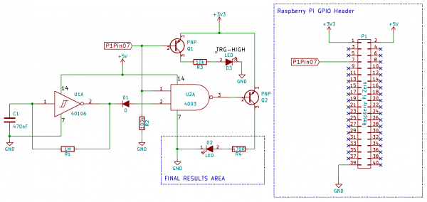
Wow, thanks for the explanation. I really appreciate your patience and time writing it out. I have been doing research on the web to learn this, but sometimes it's good to get pointed in the right direction. I was also looking at the logic level convertors at Adafruit. I put the transistors in as a learning exercise for me. The key statement that really helped was that they are "current driven" and not "voltage driven". I need to learn more about the theory behind transistors. Basically, I just hacked this until it (perceptibly) "worked" (as you can tell by all of the mistakes).
Thanks again for your help. |
|
|
Back to top
|
|
|
cerkit
Joined: Nov 17, 2016
Posts: 17
Location: Montgomery, AL USA
|
| Posted: Wed Dec 14, 2016 3:59 pm Post subject:
Re: 5v for entire circuit? |
|
|
| Blue Hell wrote: | | cerkit wrote: | | Where would the resistors go on Q1 and Q2? Also, if I switch Q1 to a 5v supply, what's the best way to protect P1Pin07 from the 5v?. |
The transistors have a fixed voltage drop from base to emitter, it depends on the base emitter current, from zero to about 0.7 Volt. So when the emitter is at a fixed voltage and the base is at a fixed voltage and the difference is over that 0.7 V an unlimited amount of current could flow (which will not happen as there are other physical constraints, like limited supply current to be available or components to go up in smoke).
In the schematic above, for example, for Q2 the emitter is fixed to 3v3, and the base can be switched from 5V to 0V. The 5V situation would reverse bias Q2, but only by 5 - 3.3 = 1v7, and it can handle that. The 0 V situation would cause a drop of 3v3, which is over the 0v7 limit, that is a nono as it would cause unlimited current to flow (which in this case will not happen as U2A can only sink a limited amount of current - hence nothing will actually blow, but it is bad design).
You can fix this by adding a resistor, either in the emitter or in the base connection. Effectively this will change the mode from voltage driven to current driven, and that is what a transistor was designed for.
In this particular case putting a resistor in the emitter connection would be troublesome, as it would affect the LED (D2), but a base resistor would solve the problem by limiting the amount of current that could flow. The base resistor would be connected from the base of Q2 to pin 3 of U2A, replacing the direct link that is there now.
For Q1 the situation is basically the same. When P1pin07 is high (and I assume that to be 3v3) all is ok, as there is no BE voltage over Q1. However when P1pin07 goes low (oV) it will try to put a voltage over 0v7 over Q1, resulting in potentially unlimited current again. Again an emitter resistor would affect the LED, but a base resistor (replacing the link from Q1's base to P1pin07) would limit the current.
In both cases a resistor of say 1 .. 10K would do it, its not very critical, there must be something though. |
OK, I made the modifications as you suggested and it seems to be working.
I took out the addditional LED (Q1 onj the original schematic) as it was causing unnecessary confusion.
This circuit seems to be working properly, but I'm not sure if I have everything in the proper place.
Even though the output voltage of Pin 7 is 3.3v, it seems to be triggering the NAND gate effectively (I checked the data sheet and the lowest voltage is right below 3.3v, but it states that it requires a 5v trigger). I don't have any AND gate IC's yet, so I need to wait until I get one.
Do you see any short circuits or design flaws with this particular schematic?
| Description: |
| This is a revision of the original schematic (that contained short circuits and errors). This schematic removed the flag indicator LED to make it simpler. |
|
| Filesize: |
37.15 KB |
| Viewed: |
324 Time(s) |
| This image has been reduced to fit the page. Click on it to enlarge. |
|
|
|
|
Back to top
|
|
|
gdavis
Joined: Feb 27, 2013
Posts: 359
Location: San Diego
Audio files: 1
|
| Posted: Wed Dec 14, 2016 4:36 pm Post subject:
|
|
|
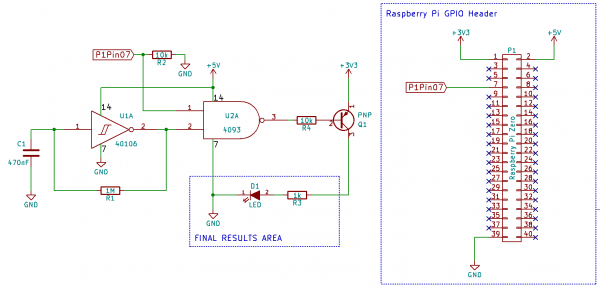
I'm a little late to the party so I haven't read the whole thread in detail, sorry if I missed something, but in your latest schematic, why the 5V instead of just putting everything on 3.3V?
Why is R2 there?
_________________
My synth build blog: http://gndsynth.blogspot.com/ |
|
|
Back to top
|
|
|
cerkit
Joined: Nov 17, 2016
Posts: 17
Location: Montgomery, AL USA
|
| Posted: Wed Dec 14, 2016 4:40 pm Post subject:
|
|
|
| gdavis wrote: | I'm a little late to the party so I haven't read the whole thread in detail, sorry if I missed something, but in your latest schematic, why the 5V instead of just putting everything on 3.3V?
Why is R2 there? |
The CMOS chips I'm using have trigger voltages of 5v and I'm driving all of my Lunetta CMOS chips at 5v.
R2 was recommended when I had a transistor on that Pinout frOm the Raspbery Pi, it may not be necessary any longer. However, when I'ts not there, pin 1 of the 4093 doe not ever go to 0v since there seems to be some signal coming through the Pin7 of the Pi when my program exits. Maybe it's floating at some unknown value. |
|
|
Back to top
|
|
|
gdavis
Joined: Feb 27, 2013
Posts: 359
Location: San Diego
Audio files: 1
|
| Posted: Wed Dec 14, 2016 5:02 pm Post subject:
|
|
|
| cerkit wrote: | | gdavis wrote: | I'm a little late to the party so I haven't read the whole thread in detail, sorry if I missed something, but in your latest schematic, why the 5V instead of just putting everything on 3.3V?
Why is R2 there? |
The CMOS chips I'm using have trigger voltages of 5v |
The trigger level should be relative to VDD, the 4093 data sheet I looked at states a minimum VDD of 3V. If you're feeding it 3.3V, you really should supply it 3.3V.
| Quote: | | and I'm driving all of my Lunetta CMOS chips at 5v. |
if you want to drive 5V out then the transistor should be on 5V, not 3.3V.
You need to decide where you want to shift your level from 3.3V to 5V. If you want to keep consistent and run all your CMOS logic at 5V (which I think is a good idea), you should level shift the output from the PI. It may seem to work now, but as you noted from the data sheet, you're right at the limit which could make it unreliable.
| Quote: | | R2 was recommended when I had a transistor on that Pinout form the Raspbery Pi, it may not be necessary any longer. However, when I'ts not there, pin 1 of the 4093 doe not ever go to 0v since there seems to be some signal coming through the Pin7 of the Pi, even when set to low. |
Hmm, if the output is actively driving high and low the resistor shouldn't be necessary for the current circuit. I suspect the output might not be configured correctly, you may want to look into that.
_________________
My synth build blog: http://gndsynth.blogspot.com/ |
|
|
Back to top
|
|
|
cerkit
Joined: Nov 17, 2016
Posts: 17
Location: Montgomery, AL USA
|
| Posted: Wed Dec 14, 2016 7:28 pm Post subject:
|
|
|
| gdavis wrote: | | cerkit wrote: | | gdavis wrote: | I'm a little late to the party so I haven't read the whole thread in detail, sorry if I missed something, but in your latest schematic, why the 5V instead of just putting everything on 3.3V?
Why is R2 there? |
The CMOS chips I'm using have trigger voltages of 5v |
The trigger level should be relative to VDD, the 4093 data sheet I looked at states a minimum VDD of 3V. If you're feeding it 3.3V, you really should supply it 3.3V.
| Quote: | | and I'm driving all of my Lunetta CMOS chips at 5v. |
if you want to drive 5V out then the transistor should be on 5V, not 3.3V.
You need to decide where you want to shift your level from 3.3V to 5V. If you want to keep consistent and run all your CMOS logic at 5V (which I think is a good idea), you should level shift the output from the PI. It may seem to work now, but as you noted from the data sheet, you're right at the limit which could make it unreliable.
| Quote: | | R2 was recommended when I had a transistor on that Pinout form the Raspbery Pi, it may not be necessary any longer. However, when I'ts not there, pin 1 of the 4093 doe not ever go to 0v since there seems to be some signal coming through the Pin7 of the Pi, even when set to low. |
Hmm, if the output is actively driving high and low the resistor shouldn't be necessary for the current circuit. I suspect the output might not be configured correctly, you may want to look into that. |
Thanks, that's basically the same conclusion I came to.
From an earlier post (I know this thread is a bit long):
| cerkit wrote: | | I have been doing research on the web to learn this, but sometimes it's good to get pointed in the right direction. I was also looking at the logic level convertors at Adafruit. I put the transistors in as a learning exercise for me. |
I'm just going to wait until I get the logic level converters and do it the correct way. My "experiments" with transistors simply taught me that I have a lot to learn about theory. I'm trying to balance my time between "hacking" and learning theory. I know there's a basic level that I need to get to so I have enough working knowledge that I don't zap all of my components or kill myself with hooking things up wrong. 
Ultimately, I do plan to graduate beyond blinky lights and actually come up with experimental applications combining CMOS Oscillators, counters, dividers, and the Raspberry Pi (plus my favorite programming language) to do interesting things with code and hardware. |
|
|
Back to top
|
|
|
|

 Forum index » DIY Hardware and Software » Lunettas - circuits inspired by Stanley Lunetta